DLPS160B April 2019 – February 2023 DLP480RE
PRODUCTION DATA
- 1 Features
- 2 Applications
- 3 Description
- 4 Revision History
- 5 Pin Configuration and Functions
-
6 Specifications
- 6.1 Absolute Maximum Ratings
- 6.2 Storage Conditions
- 6.3 ESD Ratings
- 6.4 Recommended Operating Conditions
- 6.5 Thermal Information
- 6.6 Electrical Characteristics
- 6.7 Capacitance at Recommended Operating Conditions
- 6.8 Timing Requirements
- 6.9 System Mounting Interface Loads
- 6.10 Micromirror Array Physical Characteristics
- 6.11 Micromirror Array Optical Characteristics
- 6.12 Window Characteristics
- 6.13 Chipset Component Usage Specification
- 7 Detailed Description
- 8 Application and Implementation
- 9 Power Supply Recommendations
- 10Layout
- 11Device and Documentation Support
Package Options
Mechanical Data (Package|Pins)
- FXG|257
Thermal pad, mechanical data (Package|Pins)
Orderable Information
6.8 Timing Requirements
| MIN | NOM | MAX | UNIT | |||
|---|---|---|---|---|---|---|
| SCP#DLPS1602029 | ||||||
| tr | Rise time | 20% to 80% reference points | 30 | ns | ||
| tf | Fall time | 80% to 20% reference points | 30 | ns | ||
| LVDS#DLPS1607287 | ||||||
| tr | Rise slew rate | 20% to 80% reference points | 0.7 | 1 | V/ns | |
| tf | Fall slew rate | 80% to 20% reference points | 0.7 | 1 | V/ns | |
| tC | Clock cycle | DCLK_C,LVDS pair | 2.5 | ns | ||
| DCLK_D, LVDS pair | 2.5 | ns | ||||
| tW | Pulse duration | DCLK_C LVDS pair | 1.19 | 1.25 | ns | |
| DCLK_D LVDS pair | 1.19 | 1.25 | ns | |||
| tSu | Setup time | D_C(15:0) before DCLK_C, LVDS pair | 0.275 | ns | ||
| D_D(15:0) before DCLK_D, LVDS pair | 0.275 | ns | ||||
| SCTRL_C before DCLK_C, LVDS pair | 0.275 | ns | ||||
| SCTRL_D before DCLK_D, LVDS pair | 0.275 | ns | ||||
| th | Hold time | D_C(15:0) after DCLK_C, LVDS pair | 0.195 | ns | ||
| D_D(15:0) after DCLK_D, LVDS pair | 0.195 | ns | ||||
| SCTRL_C after DCLK_C, LVDS pair | 0.195 | ns | ||||
| SCTRL_D after DCLK_D, LVDS pair | 0.195 | ns | ||||
| LVDS#DLPS1607287 | ||||||
| tSKEW | Skew time | Channel D relative to Channel C#DLPS1603235#DLPS1603802, LVDS pair | –1.25 | 1.25 | ns | |
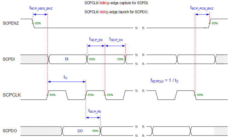
 Figure 6-2 SCP
Timing Requirements
Figure 6-2 SCP
Timing RequirementsSee Recommended Operating Conditions for fSCPCLK, tSCP_DS, tSCP_DH and tSCP_PD specifications.
See Timing Requirements for tr and tf specifications and conditions.
 Figure 6-4 Test Load
Circuit for Output Propagation Measurement
Figure 6-4 Test Load
Circuit for Output Propagation MeasurementFor output timing analysis, the tester pin electronics and its transmission line effects must be taken into account. System designers use IBIS or other simulation tools to correlate the timing reference load to a system environment.
 Figure 6-5 LVDS
Waveform Requirements
Figure 6-5 LVDS
Waveform RequirementsSee Recommended Operating Conditions for VCM, VID, and VLVDS specifications and conditions.
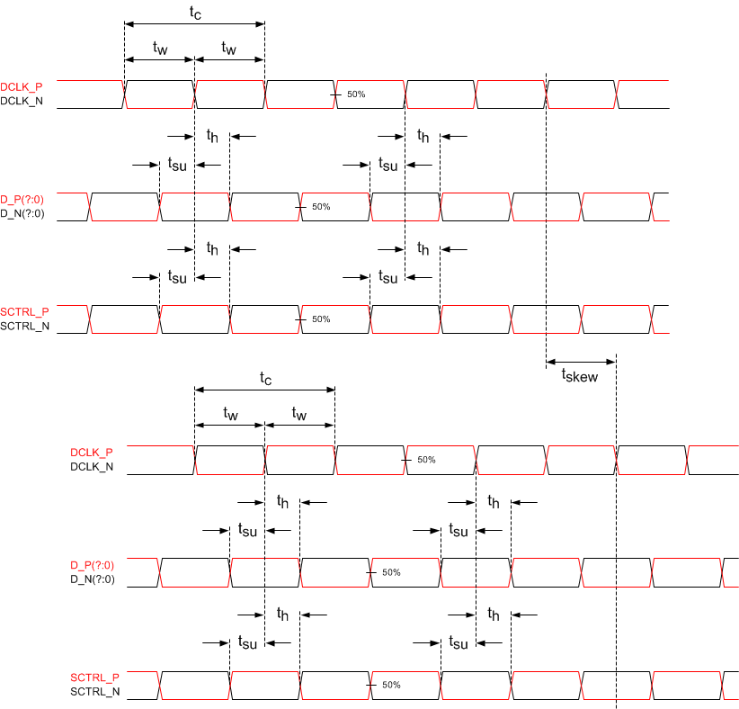
 Figure 6-6 Timing
Requirements
Figure 6-6 Timing
RequirementsSee Timing Requirements for timing requirements and LVDS pairs per channel (bus) defining D_P(?:0) and D_N(?:0).