SLCS006X October 1979 – October 2023 LM139 , LM139A , LM239 , LM239A , LM2901 , LM2901AV , LM2901B , LM2901V , LM339 , LM339A , LM339B
PRODMIX
- 1
- 1 Features
- 2 Applications
- 3 Description
- 4 Revision History
- 5 Other Versions
- 6 Pin Configuration and Functions
-
7 Specifications
- 7.1 Absolute Maximum Ratings for LM339B and LM2901B
- 7.2 Absolute Maximum Ratings for Non-B Versions
- 7.3 ESD Ratings for LM339B and LM2901B
- 7.4 ESD Ratings, Non-B Versions
- 7.5 Recommended Operating Conditions for LM339B and LM2901B
- 7.6 Recommended Operating Conditions, Non-B Versions
- 7.7 Thermal Information for LM339B and LM2901B
- 7.8 Thermal Information for Non-B Versions
- 7.9 Electrical Characteristics for LM339B
- 7.10 Electrical Characteristics for LM2901B
- 7.11 Electrical Characteristics for LM139 and LM139A
- 7.12 Electrical Characteristics for LMx39 and LMx39A
- 7.13 Electrical Characteristics for LM2901, LM2901V and LM2901AV
- 7.14 Switching Characteristics for LM139 and LM139A
- 7.15 Switching Characteristics for LM339B and LM2901B
- 7.16 Switching Characteristics for LMx39 and LMx39A
- 7.17 Switching Characteristics for LM2901
- 7.18 Typical Characteristics for LM339B and LM2901B Only
- 7.19 Typical Characteristics, Non-B Versions
- 8 Detailed Description
- 9 Application and Implementation
- 10Device and Documentation Support
- 11Mechanical, Packaging, and Orderable Information
Package Options
Refer to the PDF data sheet for device specific package drawings
Mechanical Data (Package|Pins)
- D|14
- DB|14
- PW|14
- N|14
- NS|14
Thermal pad, mechanical data (Package|Pins)
Orderable Information
7.18 Typical Characteristics for LM339B and LM2901B Only
TA = 25°C, VS = 5 V, RPULLUP = 5.1k, CL = 15 pF, VCM = 0 V, VUNDERDRIVE = 100 mV, VOVERDRIVE = 100 mV unless otherwise noted.
 Figure 7-1 Total Supply Current vs. Supply Voltage
 Figure 7-3 Total Supply Current vs. Input Voltage at 3.3V
 Figure 7-5 Total Supply Current vs. Input Voltage at 12V
 Figure 7-7 Input Offset Voltage vs. Temperature at 3V
 Figure 7-9 Input Offset Voltage vs. Temperature at 12V
 Figure 7-11 Input Offset Voltage vs. Supply Voltage at -40°C
 Figure 7-13 Input Offset Voltage vs. Supply Voltage at 85°C
 Figure 7-15 Input Bias Current vs. Supply Voltage
 Figure 7-17 Input Bias Current vs. Input Voltage at 12V
 Figure 7-19 Output Low Voltage vs. Output Sinking Current at 3V
 Figure 7-21 Output Low Voltage vs. Output Sinking Current at 12V
 Figure 7-23 Output High Leakage Current vs.Temperature at 5V
 Figure 7-25 High to Low Propagation Delay vs. Input Overdrive Voltage, 5V
 Figure 7-27 High to Low Propagation Delay vs. Input Overdrive Voltage, 12V
 Figure 7-29 High to Low Propagation Delay vs. Input Overdrive Voltage, 36V
 Figure 7-31 Response Time for Various Overdrives, High-to-Low Transition
 Figure 7-2 Total Supply Current vs. Input Voltage at 3V
 Figure 7-4 Total Supply Current vs. Input Voltage at 5V
 Figure 7-6 Total Supply Current vs. Input Voltage at 36V
 Figure 7-8 Input Offset Voltage vs. Temperature at 5V
 Figure 7-10 Input Offset Voltage vs. Temperature at 36
 Figure 7-12 Input Offset Voltage vs. Supply Voltage at 25°C
 Figure 7-14 Input Offset Voltage vs. Supply Voltage at 125°C
 Figure 7-16 Input Bias Current vs. Input Voltage at 5V
 Figure 7-18 Input Bias Current vs. Input Voltage at 36V
 Figure 7-20 Output Low Voltage vs. Output Sinking Current at 5V
 Figure 7-22 Output Low Voltage vs.Output Sinking Current at 36V
 Figure 7-24 Output High Leakage Current vs. Temperature at 36V
 Figure 7-26 Low to High Propagation Delay vs. Input Overdrive Voltage, 5V
 Figure 7-28 Low to High Propagation Delay vs. Input Overdrive Voltage, 12V
 Figure 7-30 Low to High Propagation Delay vs. Input Overdrive Voltage, 36V
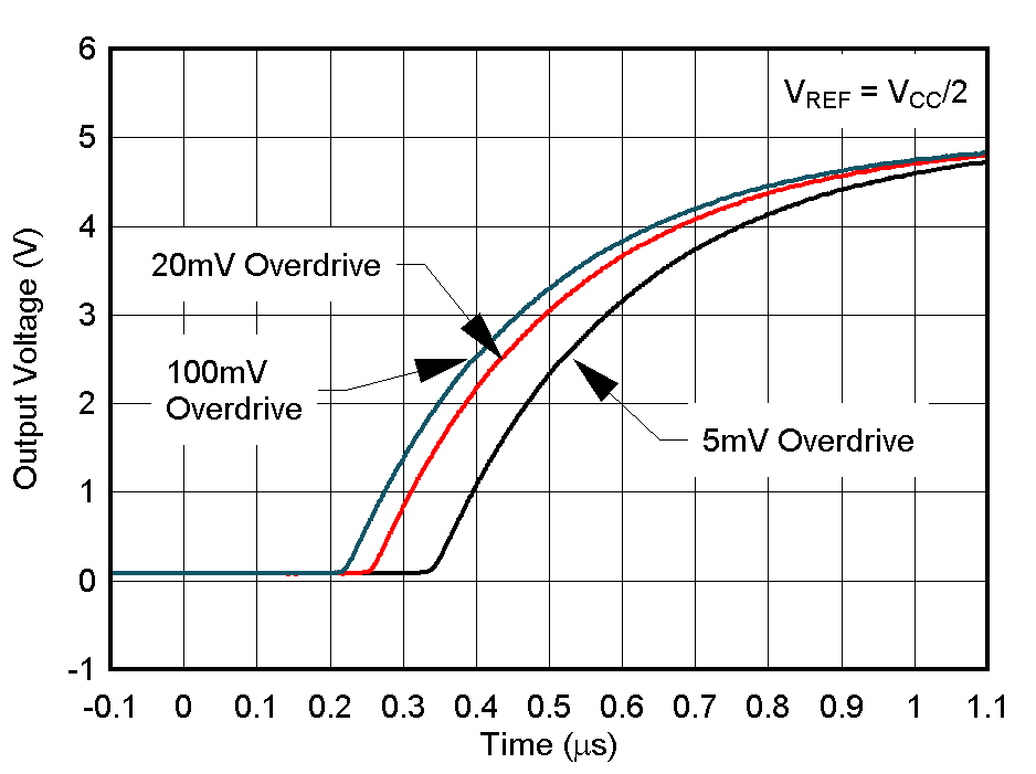
 Figure 7-32 Response Time for Various Overdrives, Low-to-High Transition