SLUSEY1B June 2023 – December 2023 LMR51606 , LMR51610
PRODUCTION DATA
- 1
- 1 Features
- 2 Applications
- 3 Description
- 4 Device Comparison Table
- 5 Pin Configuration and Functions
- 6 Specifications
- 7 Detailed Description
-
8 Application and Implementation
- 8.1 Application Information
- 8.2
Typical Application
- 8.2.1 Design Requirements
- 8.2.2
Detailed Design Procedure
- 8.2.2.1 Custom Design With WEBENCH® Tools
- 8.2.2.2 Output Voltage Setpoint
- 8.2.2.3 Switching Frequency
- 8.2.2.4 Inductor Selection
- 8.2.2.5 Output Capacitor Selection
- 8.2.2.6 Input Capacitor Selection
- 8.2.2.7 Bootstrap Capacitor
- 8.2.2.8 Undervoltage Lockout Setpoint
- 8.2.2.9 Replacing Non Sync Converter
- 8.2.3 Application Curves
- 8.3 Power Supply Recommendations
- 8.4 Layout
- 9 Device and Documentation Support
- 10Revision History
- 11Mechanical, Packaging, and Orderable Information
Package Options
Mechanical Data (Package|Pins)
- DBV|6
Thermal pad, mechanical data (Package|Pins)
Orderable Information
3 Description
The LMR516xx is a wide-VIN, easy-to-use synchronous buck converter capable of driving up to 0.6-A and 1-A load current. With a wide input range of 4 V to 65 V, the device is designed for a wide range of industrial applications for power conditioning from an unregulated source.
The LMR516xx operates at 400-kHz and 1.1-MHz switching frequency to support use of relatively small inductors for an optimized design size. The LMR516xx has a PFM version to realize high efficiency at light load and a FPWM version to achieve constant frequency and small output voltage ripple over the full load range. Soft-start and compensation circuits are implemented internally, which allow the device to be used with minimal external components.
The device has built-in protection features, such as cycle-by-cycle current limit, hiccup mode short-circuit protection, and thermal shutdown in case of excessive power dissipation.
| PART NUMBER(3) | PACKAGE(1) | PACKAGE SIZE(2) |
|---|---|---|
| LMR51610 | DBV (SOT-23, 6) | 2.90 mm × 2.80 mm |
| LMR51606 |
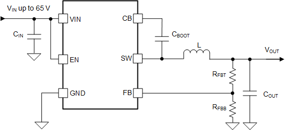
 Simplified Schematic
 Efficiency Versus Output Current
 VOUT = 5 V, 400 kHz