SBOS799E August 2019 – August 2024 OPA810
PRODUCTION DATA
- 1
- 1 Features
- 2 Applications
- 3 Description
- 4 Device Comparison Table
- 5 Pin Configuration and Functions
-
6 Specifications
- 6.1 Absolute Maximum Ratings
- 6.2 ESD Ratings
- 6.3 Recommended Operating Conditions
- 6.4 Thermal Information
- 6.5 Electrical Characteristics: 10 V
- 6.6 Electrical Characteristics: 24 V
- 6.7 Electrical Characteristics: 5 V
- 6.8 Typical Characteristics: VS = 10 V
- 6.9 Typical Characteristics: VS = 24 V
- 6.10 Typical Characteristics: VS = 5 V
- 6.11 Typical Characteristics: ±2.375-V to ±12-V Split Supply
- 7 Detailed Description
- 8 Application and Implementation
- 9 Device and Documentation Support
- 10Revision History
- 11Mechanical, Packaging, and Orderable Information
Package Options
Refer to the PDF data sheet for device specific package drawings
Mechanical Data (Package|Pins)
- D|8
- DBV|5
- DCK|5
Thermal pad, mechanical data (Package|Pins)
Orderable Information
7.3.1 OPA810 Architecture
The OPA810 features a true high-impedance input stage including a JFET differential-input pair main stage and a CMOS differential-input auxiliary (aux) stage operational within 2.5 V of the positive supply voltage. The bias current is limited to a maximum of 20 pA throughout the common-mode input range of the amplifier. Section 7.2 provides a block diagram representation for the input stage of the OPA810. The amplifier exhibits excellent performance for high-speed signals (distortion, noise, and input offset voltage) while the aux stage enables rail-to-rail inputs and prevents phase reversal. The device exhibits a CMRR and PSRR of 75 dB (typical) when the input common-mode is in aux stage.
The OPA810 also includes input clamps that enable the maximum input differential voltage of up to 7 V (lower of 7 V and total supply voltage). This architecture offers significantly greater differential input voltage capability as compared to one to two times the diode forward voltage drop maximum rating in standard amplifiers, and makes this device an excellent choice for use with multiplexers and processing of signals with fast transients. The input bias currents are also clamped to maximum 300 µA, as Figure 6-54 shows, which does not load the previous driver stage or require current-limiting resistors (except limiting current through the input ESD diodes when input common-mode voltages are greater than the supply voltages). This feature also enables this amplifier to be used as a comparator in systems that require an amplifier and a comparator for signal gain and fault detection, respectively. For the lowest offset, distortion, and noise performance, limit the common-mode input voltage to the main JFET-input stage (greater than 2.5 V away from the positive supply).
The OPA810 is a rail-to-rail output amplifier and swings to either of the rails at the output (see Figure 6-15) for 10-V supply operation. The rail-to-rail output configuration is particularly useful for inputs biased near the rails or when the amplifier is configured in a closed-loop gain such that the output approaches the supply voltage. When the output saturates, the output recovers within 55 ns when the inputs exceed the supply voltages by 0.5 V in an G = –1 V/V inverting gain with a 10–V supply. The outputs are short-circuit protected with the limits of Figure 6-16.
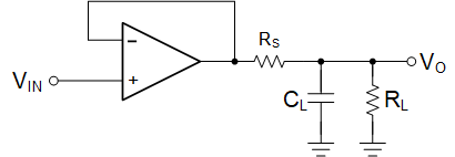
As Figure 7-1 shows, an amplifier phase margin reduces and becomes unstable when driving a capacitive load (CL) at the output. Using a series resistor (RS) between the amplifier output and load capacitance introduces a zero that cancels the pole formed by the amplifier output impedance and CL in the open-loop transfer function. The OPA810 drives capacitive loads of up to 10 pF without causing instability. Use a series resistor for larger load capacitance values, as Figure 6-3 shows for OPA810 configured as a unity-gain buffer. Figure 6-4 shows that when used in a gain larger than 1 V/V, the OPA810 is able to drive a load capacitance larger than 10 pF without the need for a series resistor at the output.
 Figure 7-1 OPA810 Driving Capacitive Load