SLLS067I August 1990 – October 2022 SN55LBC176 , SN65LBC176 , SN75LBC176
PRODUCTION DATA
- 1 Features
- 2 Description
- 3 Revision History
- 4 Description (Continued)
- 5 Pin Configuration and Functions
-
6 Specifications
- 6.1 Absolute Maximum Ratings
- 6.2 Recommended Operating Conditions
- 6.3 Thermal Information: SN55LBC176
- 6.4 Thermal Information: SN65LBC176, SN75LBC176
- 6.5 Dissipation Ratings
- 6.6 Driver Electrical Characteristics
- 6.7 Driver Switching Characteristics
- 6.8 Receiver Electrical Characteristics
- 6.9 Receiver Switching Characteristics
- 7 Parameter Measurement Information
- 8 Detailed Description
- 9 Device and Documentation Support
- 10Mechanical, Packaging, and Orderable Information
Package Options
Mechanical Data (Package|Pins)
Thermal pad, mechanical data (Package|Pins)
Orderable Information
8.2 Device Functional Modes
Table 8-1 Driver Function Tables(1)
| DRIVER | |||
|---|---|---|---|
| INPUT D | ENABLE DE | OUTPUTS | |
| A | B | ||
| H | H | H | L |
| L | H | L | H |
| X | L | Z | Z |
(1) H = high level, L = low level, ? = indeterminate, X = irrelevant, Z = high impedance (off)
Table 8-2 Receiver Function Tables(1)
| RECEIVER | |||
|---|---|---|---|
| DIFFERENTIAL INPUTS VID = VIA – VIB | ENABLE RE | OUTPUTS R | |
| VID ≥ 0.2 V | L | H | |
| –0.2 V < VID < 0.2 V | L | ? | |
| VID ≤ –0.2 V | L | L | |
| X | H | Z | |
| Open | L | H | |
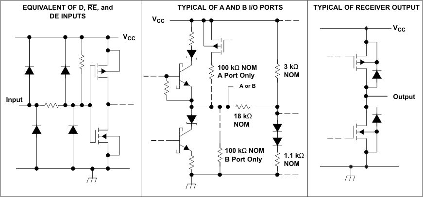
 Figure 8-3 Schematics of Inputs and Outputs