SCLS393Q APRIL 1998 – August 2015 SN74LV123A
UNLESS OTHERWISE NOTED, this document contains PRODUCTION DATA.
- 1 Features
- 2 Applications
- 3 Description
- 4 Revision History
- 5 Description (continued)
- 6 Pin Configuration and Functions
-
7 Specifications
- 7.1 Absolute Maximum Ratings
- 7.2 ESD Ratings
- 7.3 Recommended Operating Conditions
- 7.4 Thermal Information
- 7.5 Electrical Characteristics
- 7.6 Timing Requirements, VCC = 2.5 V ± 0.2 V
- 7.7 Timing Requirements, VCC = 3.3 V ± 0.3 V
- 7.8 Timing Requirements, VCC = 5 V ± 0.5 V
- 7.9 Switching Characteristics, VCC = 2.5 V ± 0.2 V
- 7.10 Switching Characteristics, VCC = 3.3 V ± 0.3 V
- 7.11 Switching Characteristics, VCC = 5 V ± 0.5 V
- 7.12 Operating Characteristics
- 7.13 Typical Characteristics
- 8 Parameter Measurement Information
- 9 Detailed Description
- 10Application and Implementation
- 11Power Supply Recommendations
- 12Layout
- 13Device and Documentation Support
- 14Mechanical, Packaging, and Orderable Information
Package Options
Mechanical Data (Package|Pins)
Thermal pad, mechanical data (Package|Pins)
- RGY|16
Orderable Information
9 Detailed Description
9.1 Overview
The SNx4LV123A devices contain two independent monostable multivibrators. They produce a specific width high output pulse when triggered (Q is normally high, pulse is low). The device uses an external RC circuit to determine the output pulse length, which is explained in detail in the Application Information section.
Pulse triggering occurs at a particular voltage level and is not directly related to the transition time of the input pulse. The A, B, and CLR inputs have Schmitt triggers with sufficient hysteresis to handle slow input transition rates with jitter-free triggering at the outputs.
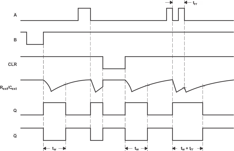
Once triggered, the basic pulse duration can be extended by retriggering the gated low-level-active (A) or high-level-active (B) input. Pulse duration can be reduced by taking CLR low. The Figure 7 illustrates pulse control by retriggering the inputs and early clearing.
During power-up, Q outputs are in the low state, and Q outputs are in the high state. The outputs are glitch free, without applying a reset pulse.
These devices are fully specified for partial-power-down applications using Ioff. The Ioff circuitry disables the outputs, preventing damaging current backflow through the device when it is powered down.
Pin assignments for these devices are identical to those of the 'AHC123A and 'AHCT123A devices for interchangeability, when allowed.
9.2 Functional Block Diagrams
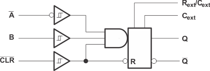
 Figure 6. Logic Diagram, Each Multivibrator (Positive Logic)
 Figure 7. Input and Output Timing Diagram
9.3 Feature Description
The 'LV123A devices operate over a wide supply range from 2 V to 5.5 V. The propagation delay has a maximum of 11 ns at 5-V supply. The typical output ground bounce is less than 0.8 V at 3.3-V supply and 25°C. The typical output VOH undershoot is greater than 2.3 V at 3.3-V supply and 25°C.
These parts support mixed-mode voltage operation on all ports.
Schmitt-trigger circuitry on the A, B, and CLR inputs allow for slow input transition rates and noisy input signals.
This device can be configured for rising or falling edge triggering.
This device supports partial-power-down mode operation.
This device is retriggerable for very long output pulses up to 100% duty cycle.
The clear signal overrides an output pulse and terminates it early.
Glitch-free power-up reset on outputs.
9.4 Device Functional Modes
Table 1 lists the functional modes of the 'LV123A devices.
Table 1. Function Table
(Each Multivibrator)
| INPUTS | OUTPUTS | |||
|---|---|---|---|---|
| CLR | A | B | Q | Q |
| L | X | X | L | H |
| X | H | X | L | H |
| X | X | L | L | H |
| H | L | ↑ |  |
 |
| H | ↓ | H |  |
 |
| ↑ | L | H |  |
 |