SBFS022C June 2003 – October 2015 SRC4192 , SRC4193
PRODUCTION DATA.
- 1 Features
- 2 Applications
- 3 Description
- 4 Revision History
- 5 Pin Configuration and Functions
- 6 Specifications
- 7 Detailed Description
- 8 Application and Implementation
- 9 Power Supply Recommendations
- 10Layout
- 11Device and Documentation Support
- 12Mechanical, Packaging, and Orderable Information
Package Options
Refer to the PDF data sheet for device specific package drawings
Mechanical Data (Package|Pins)
- DB|28
Thermal pad, mechanical data (Package|Pins)
Orderable Information
8 Application and Implementation
NOTE
Information in the following applications sections is not part of the TI component specification, and TI does not warrant its accuracy or completeness. TI’s customers are responsible for determining suitability of components for their purposes. Customers should validate and test their design implementation to confirm system functionality.
8.1 Application Information
This section of the data sheet provides practical applications information for hardware and systems engineers designing the SRC4192 and SRC4193 devices into the end equipment.
8.1.1 Interfacing to Digital Audio Receivers and Transmitters
The input and output ports of the SRC4192 and SRC4193 devices are designed to interface to a variety of audio devices, including receivers and transmitters commonly used for AES/EBU, S/PDIF, and CP1201 communications.
Texas Instruments manufactures the DIR1703 digital audio interface receiver and DIT4096/4192 digital audio transmitters to address these applications.
Figure 70 shows interfacing the DIR1703 device to the input port of the SRC4192 or SRC4193 device. The DIR1703 device operates from a single 3.3-V supply, which requires the VIO supply (pin 7) for the SRC4192 or SRC4193 device to be set to 3.3 V for interface compatibility.
 Figure 70. Interfacing the SRC4193 to the DIR1703 Digital Audio Interface Receiver
Figure 71 shows the interface between the output port of the SRC4192 or SRC4193 device and the audio serial port of the DIT4096 or DIT4192 device. Again, the VIO supplies for both the SRC419x device and DIT4096/4192 device are set to 3.3 V for compatibility.
 Figure 71. Interfacing the SRC4193 to the DIT4096/4192 Digital Audio Interface Transmitter
Like the output port of the SRC4192 or SRC4193 device, the audio serial port of the DIT4096 and DIT4192 device can be configured as a master or slave. In cases where the output port of the SRC419x device is set to master mode, use the reference clock source (RCKI) as the master clock source (MCLK) for the DIT4096/4192 device, to ensure that the transmitter is synchronized to the output port data of the SRC419x device.
8.1.2 TDM Applications
The SRC4192 and SRC4193 devices support a TDM output mode, which allows multiple devices to be daisy-chained together to create a serial frame. Each device occupies one subframe within a frame, and each sub-frame carries two channels (Left followed by Right). Each sub-frame is 64 bits long, with 32 bits allotted for each channel. The audio data for each channel is left justified within the allotted 32 bits. Figure 72 shows the TDM frame format, while Figure 73 shows TDM input timing parameters, which are listed in Electrical Characteristics.
 Figure 72. TDM Frame Format
 Figure 73. Input Timing for TDM Mode
The frame rate is equal to the output sampling frequency, fs. The BCKO frequency for the TDM interface is N × 64fs, where N is the number of devices included in the daisy chain. For Master mode, the output BCKO frequency is fixed to the reference clock (RCKI) input frequency. The number of devices that can be daisy-chained in TDM mode is dependent upon the output sampling frequency and the BCKO frequency, leading to the following numerical relationship:
where
- fBCKO = Output Port Bit Clock (BCKO), 27.648-MHz maximum
- fs = Output Port Sampling (or LRCKO) Frequency, 216-kHz maximum.
This relationship holds true for both slave and master modes.
Figure 74 and Figure 75 show typical connection schemes for TDM mode. Although the TMS320C671x DSP device family is shown as the audio processing engine in these figures, other TI digital signal processors with a multi-channel buffered serial port (McBSPTM) may also function with this arrangement. Interfacing to processors from other manufacturers is also possible. Refer to Figure 62 in this data sheet, along with the equivalent serial port timing diagrams shown in the DSP data sheet, to determine compatibility.
 Figure 74. TDM Interface where all Devices are Slaves
 Figure 75. TDM Interface where one Device is Master to Multiple Slaves
8.2 Typical Application
Figure 76 and Figure 77 show typical connection diagrams for the SRC4192 and SRC4193 devices (respectively). Recommended values for power supply bypass capacitors are included. These capacitors should be placed as close to the IC package as possible.
 Figure 76. Typical Connection Diagram for the SRC4192
 Figure 77. Typical Connection Diagram for the SRC4193
8.2.1 Design Requirements
The following lists design requirements:
- Control: Hardware, I2C, or SPI
- Audio input: PCM serial data
- Audio output: PCM serial data
- Reference clock
8.2.2 Detailed Design Procedure
8.2.2.1 Control Method
The SRC4192 is a hardware controlled device while the SRC4193 is a software controlled device. The SRC4192 control pins can be connected to VDD or GND directly or by the GPIO of a host controller. The SRC4193 can communicate over a 3 wire SPI.
8.2.2.2 Audio Input and Output
The Audio input and output ports can handle 16, 18, 20, or 24 bit right justified PCM serial data as well as 24 bit I2S or left justified PCM serial data at up to a 212-kHz sampling rate. A TDM format is also available. Both input and output can operate in slave mode, or one can operate as master while the other operates as a slave. A 16:1 or 1:16 is the max ratio supported between the input and output audio sampling rates.
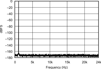
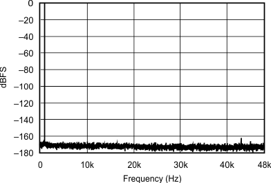
8.2.3 Application Curves

| 44.1 kHz:48 kHz | ||

| 44.1 kHz:96 kHz | ||