SLVSB67C November 2011 – June 2017 TLV70012-Q1 , TLV70018-Q1
PRODUCTION DATA.
- 1 Features
- 2 Applications
- 3 Description
- 4 Revision History
- 5 Pin Configuration and Functions
- 6 Specifications
- 7 Detailed Description
- 8 Application and Implementation
- 9 Power Supply Recommendations
- 10Layout
- 11Device and Documentation Support
- 12Mechanical, Packaging, and Orderable Information
Package Options
Mechanical Data (Package|Pins)
- DDC|5
Thermal pad, mechanical data (Package|Pins)
Orderable Information
7 Detailed Description
7.1 Overview
The TLV70018-Q1 and TLV70012-Q1 low-dropout (LDO) linear regulators are low-quiescent-current devices with excellent line and load transient performance. These LDOs are designed for power-sensitive applications. A precision bandgap and error amplifier provides overall 2% accuracy together with low output noise, very high power-supply rejection ratio (PSRR), and low dropout voltage.
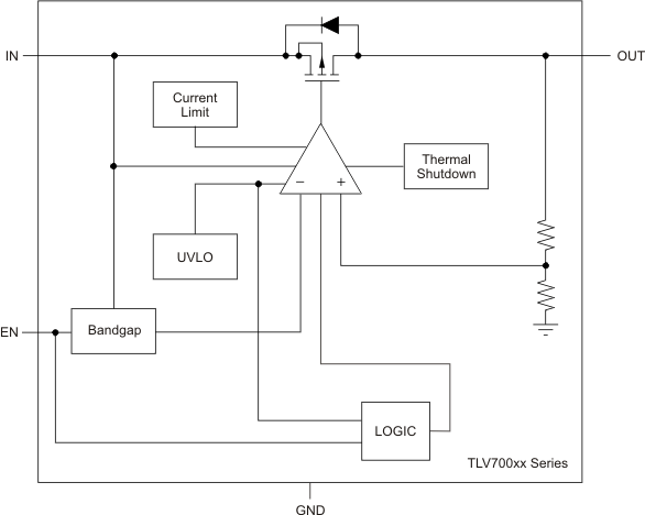
7.2 Functional Block Diagrams

7.3 Feature Description
7.3.1 Internal Current Limit
The TLV70018-Q1 and TLV70012-Q1 internal current limit helps to protect the regulator during fault conditions. During current limit, the output sources a fixed amount of current that is largely independent of the output voltage. In such a case, the output voltage is not regulated, and is VOUT = ILIMIT × RLOAD. The PMOS pass transistor dissipates (VIN – VOUT) × ILIMIT until thermal shutdown is triggered and the device turns off. As the device cools, it is turned on by the internal thermal shutdown circuit. If the fault condition continues, the device cycles between current limit and thermal shutdown. See the Thermal Considerations section for more details.
The PMOS pass element in the TLV70018-Q1 and TLV70012-Q1 has a built-in body diode that conducts current when the voltage at OUT exceeds the voltage at IN. This current is not limited, so if extended reverse voltage operation is anticipated, external limiting to 5% of the rated output current is recommended.
7.3.2 Dropout Voltage
The TLV70018-Q1 and TLV70012-Q1 use a PMOS pass transistor to achieve low dropout. When (VIN – VOUT) is less than the dropout voltage (VDO), the PMOS pass device is in the linear region of operation and the input-to-output resistance is the RDS(ON) of the PMOS pass element. VDO scales approximately with output current because the PMOS device behaves as a resistor in dropout.
As with any linear regulator, PSRR and transient response are degraded as (VIN – VOUT) approaches dropout. Figure 11 illustrates this effect.
7.3.3 Undervoltage Lockout (UVLO)
The TLV70018-Q1 and TLV70012-Q1 use an undervoltage lockout circuit to keep the output shut off until internal circuitry is operating properly.
7.3.4 Thermal Shutdown
Thermal protection disables the output when the junction temperature rises to approximately 165°C, allowing the device to cool. When the junction temperature cools to approximately 145°C, the output circuitry is again enabled. Depending on power dissipation, thermal resistance, and ambient temperature, the thermal protection circuit may cycle on and off. This cycling limits the dissipation of the regulator, protecting it from damage as a result of overheating.
Any tendency to activate the thermal protection circuit indicates excessive power dissipation or an inadequate heatsink. For reliable operation, junction temperature should be limited to 125°C maximum. To estimate the margin of safety in a complete design (including heatsink), increase the ambient temperature until the thermal protection is triggered; use worst-case loads and signal conditions. For good reliability, thermal protection should trigger at least 40°C above the maximum expected ambient condition of the particular application. This configuration produces a worst-case junction temperature of 125°C at the highest expected ambient temperature and worst-case load.
The internal protection circuitry of the TLV70018-Q1 and TLV70012-Q1 has been designed to protect against overload conditions. It was not intended to replace proper heatsinking. Continuously running the TLV70018-Q1 or TLV70012-Q1 into thermal shutdown degrades device reliability.
7.4 Device Functional Modes
7.4.1 Shutdown
The enable pin (EN) is active high. The device is enabled when voltage at EN pin goes above 0.9 V. This relatively lower value of voltage required to turn the LDO on can be exploited to power the LDO with a GPIO of recent processors whose GPIO Logic 1 voltage level is lower than traditional microcontrollers. The device is turned off when the EN pin is held at less than 0.4 V. When shutdown capability is not required, EN can be connected to the IN pin.
7.4.2 Operation with VIN Less than 2 V
The TLV70018-Q1 and TLV70012-Q1 devices operate with input voltages above 2 V. The typical UVLO voltage is 1.9 V and the device operates at an input voltage above 2 V. When input voltage falls below UVLO voltage, the device will shutdown.
7.4.3 Operation with VIN Greater than 2 V
When VIN is greater than 2 V, if input voltage is higher than desired output voltage plus dropout voltage, the output voltage is equal to the desired value. Otherwise, output voltage will be VIN minus dropout voltage.