SLVSGU2E February   2023  – April 2024 TLV709

PRODUCTION DATA  

  1.   1
  2. Features
  3. Applications
  4. Description
  5. Pin Configuration and Functions
  6. Specifications
    1. 5.1 Absolute Maximum Ratings
    2. 5.2 ESD Ratings
    3. 5.3 Recommended Operating Conditions
    4. 5.4 Thermal Information
    5. 5.5 Electrical Characteristics
    6. 5.6 Typical Characteristics
  7. Detailed Description
    1. 6.1 Overview
    2. 6.2 Functional Block Diagrams
    3. 6.3 Feature Description
      1. 6.3.1 Wide Supply Range
      2. 6.3.2 Low Quiescent Current
      3. 6.3.3 Dropout Voltage (VDO)
      4. 6.3.4 Current Limit
      5. 6.3.5 Leakage Null Control Circuit
    4. 6.4 Device Functional Modes
      1. 6.4.1 Normal Operation
      2. 6.4.2 Dropout Operation
  8. Application and Implementation
    1. 7.1 Application Information
    2. 7.2 Typical Application
      1. 7.2.1 Design Requirements
      2. 7.2.2 Detailed Design Procedure
        1. 7.2.2.1 Setting VOUT for the TLV70901 Adjustable LDO
        2. 7.2.2.2 External Capacitor Requirements
        3. 7.2.2.3 Input and Output Capacitor Requirements
        4. 7.2.2.4 Reverse Current
        5. 7.2.2.5 Feed-Forward Capacitor (CFF)
        6. 7.2.2.6 Power Dissipation (PD)
        7. 7.2.2.7 Estimating Junction Temperature
    3. 7.3 Best Design Practices
    4. 7.4 Power Supply Recommendations
    5. 7.5 Layout
      1. 7.5.1 Layout Guidelines
        1. 7.5.1.1 Power Dissipation
      2. 7.5.2 Layout Examples
  9. Device and Documentation Support
    1. 8.1 Device Support
      1. 8.1.1 Development Support
        1. 8.1.1.1 Evaluation Module
        2. 8.1.1.2 Spice Models
      2. 8.1.2 Device Nomenclature
    2. 8.2 Documentation Support
      1. 8.2.1 Related Documentation
    3. 8.3 Receiving Notification of Documentation Updates
    4. 8.4 Support Resources
    5. 8.5 Trademarks
    6. 8.6 Electrostatic Discharge Caution
    7. 8.7 Glossary
  10. Revision History
  11. 10Mechanical, Packaging, and Orderable Information

Package Options

Mechanical Data (Package|Pins)
Thermal pad, mechanical data (Package|Pins)
Orderable Information

Setting VOUT for the TLV70901 Adjustable LDO

As illustrated in Figure 7-2, the TLV709 contains an adjustable version (the TLV70901) that sets the output voltage using an external resistor divider. The output voltage operating range is 1.2V to 28V, and is calculated using:
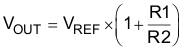
Equation 2. GUID-F157BB73-A33E-4596-AB69-A4897868B34C-low.gif

where:

  • VREF = 1.205V (typical)

Choose resistors R1 and R2 to allow approximately 1.5μA of current through the resistor divider. Lower value resistors provide improved noise performance, but consume more power. Avoid higher resistor values. Leakage current into or out of FB across R1 / R2 creates an offset voltage proportional to VOUT divided by VREF. The recommended design procedure is to choose R2 = 1MΩ to set the divider current at 1.5μA, and then calculate R1 using Equation 3:

Equation 3. R1 = VOUTVREF - 1×R2

Figure 7-2 depicts this configuration.