SLVSES2J August 2018 – May 2021 TLV803E , TLV809E , TLV810E
PRODMIX
- 1 Features
- 2 Applications
- 3 Description
- 4 Revision History
- 5 Device Comparison
- 6 Pin Configuration and Functions
- 7 Specifications
- 8 Detailed Description
- 9 Application and Implementation
- 10Power Supply Recommendations
- 11Layout
- 12Device and Documentation Support
- 13Mechanical, Packaging, and Orderable Information
Package Options
Mechanical Data (Package|Pins)
Thermal pad, mechanical data (Package|Pins)
- DPW|5
Orderable Information
8.3.3 VDD Glitch Immunity
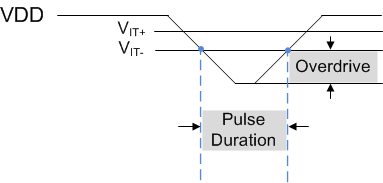
These devices are immune to quick voltage transient or excursion on VDD. Sensitivity to transients depends on both pulse duration (tGI) found in Section 7.6 and transient overdrive. Overdrive is defined by how much VDD exceeds the specified threshold. Threshold overdrive is calculated as a percent of the threshold in question, as shown in Equation 1.
where
- VIT– is the threshold voltage
- VDD is the input voltage crossing VIT–
 Figure 8-1 Overdrive Versus Pulse Duration
TLV803E, TLV809E, and TLV810E devices have
built-in glitch immunity (tGI) of 10 µs typical as shown in
Section 7.6.
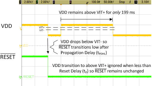
Figure 8-2 shows that VDD must fall below VIT- for tGI, otherwise the faling
transistion is ignored. When VDD falls below VIT- for tGI,
RESET transitions low to indicate a fault condition after the
propagation delay high-to-low (tPDHL). When VDD rises above VIT+,
RESET only deasserts to logic high indicating there is no more fault
condition only if VDD remains above VIT+ for longer than the reset delay
(tD).
 Figure 8-2 Glitch Immunity when VDD Rises Above VIT+ for Less than
RESET Delay (TLV803EA29)