SLVSCH2 July 2014 TPS2105-EP
PRODUCTION DATA.
- 1 Features
- 2 Applications
- 3 Description
- 4 Revision History
- 5 Pin Configuration and Functions
- 6 Specifications
- 7 Detailed Description
- 8 Application and Implementation
- 9 Power Supply Recommendations
- 10Layout
- 11Device and Documentation Support
- 12Mechanical, Packaging, and Orderable Information
Package Options
Mechanical Data (Package|Pins)
- DBV|5
Thermal pad, mechanical data (Package|Pins)
Orderable Information
8 Application and Implementation
8.1 Application Information
The TPS2105 is a dual-input, single-output power switch designed to provide uninterrupted output voltage when transitioning between two independent power supplies.
8.2 Typical Application
 Figure 15. Typical Application Schematic
8.2.1 Design Requirements
For this design example, use the following as the input parameters.
Table 1. Design Parameters
| DESIGN PARAMETER | EXAMPLE VALUE |
|---|---|
| Input voltage range, VI(IN1) | 5 V |
| Input voltage range, VI(IN2) | 5 V |
| Output voltage | 5 V |
| Continuous output current, IO | 100 mA |
| Output capacitor, CL | 220 µF |
8.2.2 Detailed Design Procedure
8.2.2.1 Step-by-Step Design Procedure
To begin the design process, the designer must decide upon a few parameters. The designer needs to know the following:
- Input voltage range, VI(IN1)
- Input voltage range, VI(IN2)
- Output voltage
- Continuous output current
- Output capacitance
8.2.2.2 Power-Supply Considerations
TI recommends a 0.22-µF ceramic bypass capacitor between IN and GND, close to the device. The output capacitor should be chosen based on the size of the load during the transition of the switch. TI recommends a 220-µF capacitor for 100-mA loads. Typical output capacitors (xx µF, shown in Figure 15) required for a given load can be determined from Figure 7, which shows the output voltage droop when output is switched from IN2 to IN1. The output voltage droop is insignificant when output is switched from IN1 to IN2. Additionally, bypassing the output with a 1-µF ceramic capacitor improves the immunity of the device to short-circuit transients.
8.2.2.3 Switch Transition
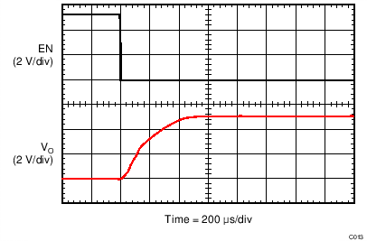
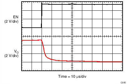
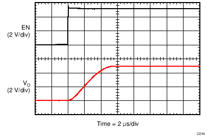
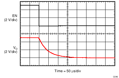
The N-channel MOSFET on IN1 uses a charge pump to create the gate-drive voltage, which gives the IN1 switch a rise time of approximately 0.4 ms. The P-channel MOSFET on IN2 has a simpler drive circuit that allows a rise time of approximately 4 µs. Because the device has two switches and a single enable pin, these rise times are seen as transition times, from IN1 to IN2, or IN2 to IN1, by the output. The controlled transition times help limit the surge currents seen by the power supply during switching.
8.2.2.4 Thermal Protection
Thermal protection provided on the IN1 switch prevents damage to the IC when heavy-overload or short-circuit faults are present for extended periods of time. The increased dissipation causes the junction temperature to rise to dangerously high levels. The protection circuit senses the junction temperature of the switch and shuts it off at approximately 145°C (TJ). The switch remains off until the junction temperature has dropped approximately 10°C. The switch continues to cycle in this manner until the load fault or input power is removed.
8.2.2.5 Undervoltage Lockout
An undervoltage lockout function is provided to ensure that the power switch is in the off state at power-up. Whenever the input voltage falls below approximately 2 V, the power switch quickly turns off. This function facilitates the design of hot-insertion systems that may not have the capability to turn off the power switch before input power is removed. Upon reinsertion, the power switch is turned on with a controlled rise time to reduce EMI and voltage overshoots.
8.2.2.6 Power Dissipation and Junction Temperature
The low on-resistance on the N-channel MOSFET allows small surface-mount packages, such as SOIC, to pass large currents. The thermal resistances of these packages are high compared to those of power packages; it is a good design practice to check power dissipation and junction temperature. First, find ron at the input voltage and operating temperature. As an initial estimate, use the highest operating ambient temperature of interest and read ron from Figure 13 or Figure 14. Next calculate the power dissipation using:
Finally, calculate the junction temperature:
where
- TA = Ambient temperature
- RθJA = Thermal resistance
Compare the calculated junction temperature with the initial estimate. If they do not agree within a few degrees, repeat the calculation using the calculated value as the new estimate. Two or three iterations are generally sufficient to obtain a reasonable answer.
8.2.2.7 ESD Protection
All TPS2105 pins incorporate ESD-protection circuitry designed to withstand a 2-kV human-body-model, 750-V CDM, and 200-V machine-model discharge as defined in MIL-STD-883C.
8.2.3 Application Curves

| VI(IN1) = 0 V | VI(IN2) = 5 V | CL = 1 µF |
| RL = 50 Ω | ||
1-µF Load, IN2 Turnon

| VI(IN1) = 0 V | VI(IN2) = 5 V | CL = 1 µF |
| RL = 50 Ω | ||
1-µF Load, IN2 Turnoff

| VI(IN1) = 5 V | VI(IN2) = 0 V | CL = 1 µF |
| RL = 50 Ω | ||
1-µF Load, IN1 Turnon

| VI(IN1) = 5 V | VI(IN2) = 0 V | CL = 1 µF |
| RL = 50 Ω | ||
1-µF Load, IN1 Turnoff