SLVSBH4F June 2012 – July 2016 TPS22966
PRODUCTION DATA.
- 1 Features
- 2 Applications
- 3 Description
- 4 Revision History
- 5 Pin Configuration and Functions
- 6 Specifications
- 7 Parameter Measurement Information
- 8 Detailed Description
- 9 Application and Implementation
- 10Power Supply Recommendations
- 11Layout
- 12Device and Documentation Support
- 13Mechanical, Packaging, and Orderable Information
Package Options
Mechanical Data (Package|Pins)
- DPU|14
Thermal pad, mechanical data (Package|Pins)
- DPU|14
Orderable Information
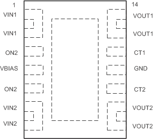
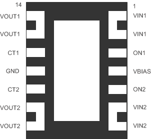
5 Pin Configuration and Functions
DPU Package
14-Pin WSON
Top View

DPU Package
14-Pin WSON
Bottom View

Pin Functions
| PIN | TYPE | DESCRIPTION | |
|---|---|---|---|
| NO. | NAME | ||
| 1 | VIN1 | I | Switch 1 input. Recommended voltage range for this pin for optimal RON performance is 0.8 V to VBIAS. Place an optional decoupling capacitor between this pin and GND for reduce VIN dip during turnon of the channel. See the Application Information section for more information |
| 2 | VIN1 | I | Switch 1 input. Recommended voltage range for this pin for optimal RON performance is 0.8 V to VBIAS. Place an optional decoupling capacitor between this pin and GND for reduce VIN dip during turnon of the channel. See the Application Information section for more information |
| 3 | ON1 | I | Active high switch 1 control input. Do not leave floating |
| 4 | VBIAS | I | Bias voltage. Power supply to the device. Recommended voltage range for this pin is 2.5 V to 5.5 V. See the Application Information section |
| 5 | ON2 | I | Active high switch 2 control input. Do not leave floating |
| 6 | VIN2 | I | Switch 2 input. Recommended voltage range for this pin for optimal RON performance is 0.8 V to VBIAS. Place an optional decoupling capacitor between this pin and GND for reduce VIN dip during turnon of the channel. See the Application Information section for more information |
| 7 | VIN2 | I | Switch 2 input. Recommended voltage range for this pin for optimal RON performance is 0.8 V to VBIAS. Place an optional decoupling capacitor between this pin and GND for reduce VIN dip during turnon of the channel. See the Application Information section for more information |
| 8 | VOUT2 | O | Switch 2 output |
| 9 | VOUT2 | O | Switch 2 output |
| 10 | CT2 | O | Switch 2 slew rate control. Can be left floating. Capacitor used on this pin mudt be rated for a minimum of 25 V for desired rise time performance |
| 11 | GND | — | Ground |
| 12 | CT1 | O | Switch 1 slew rate control. Can be left floating. Capacitor used on this pin must be rated for a minimum of 25 V for desired rise time performance |
| 13 | VOUT1 | O | Switch 1 output |
| 14 | VOUT1 | O | Switch 1 output |
| — | Thermal Pad | — | Thermal pad (exposed center pad) to alleviate thermal stress. Tie to GND. See the Layout section for layout guidelines |