SLVSAD5A July 2010 – August 2015 TPS62120 , TPS62122
PRODUCTION DATA.
- 1 Features
- 2 Applications
- 3 Description
- 4 Revision History
- 5 Device Comparison Table
- 6 Pin Configuration and Functions
- 7 Specifications
- 8 Detailed Description
- 9 Application and Implementation
- 10Power Supply Recommendations
- 11Layout
- 12Device and Documentation Support
- 13Mechanical, Packaging, and Orderable Information
Package Options
Mechanical Data (Package|Pins)
- DRV|6
Thermal pad, mechanical data (Package|Pins)
- DRV|6
Orderable Information
9 Application and Implementation
NOTE
Information in the following applications sections is not part of the TI component specification, and TI does not warrant its accuracy or completeness. TI’s customers are responsible for determining suitability of components for their purposes. Customers should validate and test their design implementation to confirm system functionality.
9.1 Application Information
The TPS6212x device is a highly efficient synchronous step-down DC-DC converter optimized for low-power applications. With its wide input voltage range, the device also fits for energy harvesting applications to convert electrical power from electromagnetic transducers.
9.2 Typical Applications
9.2.1 TPS62120 With Open-Drain Output
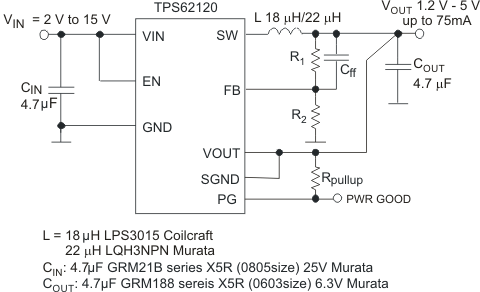 Figure 7. Standard Circuit for TPS62120 With Open-Drain Output
9.2.1.1 Design Requirements
The device operates over an input voltage range from 2 V to 15V. The output voltage is adjustable using an external feedback divider network.
The design guideline provides a component selection to operate the device within the Recommended Operating Conditions.
9.2.1.2 Detailed Design Procedure
9.2.1.2.1 Output Voltage Setting
The output voltage can be calculated to:

To minimize the current through the feedback divider network, R2 should be within the range of 82 kΩ to 360 kΩ. The sum of R1 and R2 should not exceed approximately 1 MΩ, to keep the network robust against noise. An external feedforward capacitor Cff is required for optimum regulation performance. R1 and Cff places a zero in the feedback loop.

The value for Cff can be calculated as:

Table 1 shows a selection of suggested values for the feedback divider network for most common output voltages.
Table 1. Suggested Values for Feedback Divider Network
| VOLTAGE SETTING (V) | 3.06 | 3.29 | 2.00 | 1.80 | 1.20 | 5.00 |
|---|---|---|---|---|---|---|
| R1 [kΩ] | 510 | 560 | 360 | 300 | 180 | 430 |
| R2 [kΩ] | 180 | 180 | 240 | 240 | 360 | 82 |
| Cff [pF] | 15 | 22 | 22 | 22 | 27 | 15 |
9.2.1.2.2 Output Filter Design (Inductor and Output Capacitor)
The TPS6212x operates with effective inductance values in the range of 10 µH to 33 µH and with effective output capacitance in the range of 1 µF to 33 µF. The device is optimized to operate for an output filter of L = 22 µH and COUT = 4.7 µF. Larger or smaller inductor and capacitor values can be used to optimize the performance of the device for specific operation conditions. For more details, see Checking Loop Stability.
9.2.1.2.3 Inductor Selection
The inductor value affects its peak-to-peak ripple current, the PWM-to-PFM transition point, the output voltage ripple, and the efficiency. The selected inductor has to be rated for its DC resistance and saturation current. The inductor ripple current (ΔIL) decreases with higher inductance and increases with higher VIN or VOUT and can be estimated according to Equation 8.
Equation 9 calculates the maximum inductor current under static load conditions. The saturation current of the inductor should be rated higher than the maximum inductor current as calculated with Equation 9. This is recommended because during heavy load transient the inductor current will rise above the calculated value. A more conservative way is to select the inductor saturation current according to the high-side MOSFET switch current limit ILIMF.


where
- TON = See Equation 1
- L = Inductor value
- ΔIL = Peak-to-peak inductor ripple current
- ILmax = Maximum inductor current
In DC-DC converter applications, the efficiency is essentially affected by the inductor AC resistance (that is, quality factor) and by the inductor DCR value. To achieve high efficiency operation, care should be taken in selecting inductors featuring a quality factor above 25 at the switching frequency. Increasing the inductor value produces lower RMS currents, but degrades transient response. For a given physical inductor size, increased inductance usually results in an inductor with lower saturation current.
The total losses of the coil consist of both the losses in the DC resistance (R(DC)) and the following frequency-dependent components:
- the losses in the core material (magnetic hysteresis loss, especially at high switching frequencies)
- additional losses in the conductor from the skin effect (current displacement at high frequencies)
- magnetic field losses of the neighboring windings (proximity effect)
- radiation losses
The following inductor series from different suppliers have been used with the TPS6212x converters.
Table 2. List of Inductors
| INDUCTANCE (µH) | DIMENSIONS (mm3) | INDUCTOR TYPE | SUPPLIER |
|---|---|---|---|
| 22 | 3 × 3 × 1.5 | LQH3NPN | Murata |
| 18/22 | 3 × 3 × 1.5 | LPS3015 | Coilcraft |
9.2.1.2.4 Output Capacitor Selection
The unique hysteretic PFM/PWM control scheme of the TPS6212x allows the use of ceramic capacitors. Ceramic capacitors with low ESR values have the lowest output voltage ripple and are recommended. The output capacitor requires either an X7R or X5R dielectric. Y5V and Z5U dielectric capacitors, aside from their wide variation in capacitance over temperature, become resistive at high frequencies.
At light load currents the converter operates in power save mode and the output voltage ripple is dependent on the output capacitor value and the PFM peak inductor current. Higher output capacitor values minimize the voltage ripple in PFM mode and tighten DC output accuracy in PFM mode.
9.2.1.2.5 Input Capacitor Selection
Because of the nature of the buck converter having a pulsating input current, a low ESR input capacitor is required for best input voltage filtering and minimizing the interference with other circuits caused by high input voltage spikes. For most applications a 4.7 µF to 10 µF ceramic capacitor is recommended. The voltage rating and DC bias characteristic of ceramic capacitors need to be considered. The input capacitor can be increased without any limit for better input voltage filtering.
For specific applications like energy harvesting a tantalum or tantalum polymer capacitor can be used to achieve a specific DC-DC converter input capacitance. Tantalum capacitors provide much better DC bias performance compared to ceramic capacitors. In this case a 1-µF or 2.2-µF ceramic capacitor should be used in parallel to provide low ESR.
Take care when using only small ceramic input capacitors. When a ceramic capacitor is used at the input and the power is being supplied through long wires, such as from a wall adapter, a load step at the output or VIN step on the input can induce large ringing at the VIN pin. This ringing can couple to the output and be mistaken as loop instability or could even damage the part by exceeding the maximum ratings.
Table 3 shows a list of input and output capacitors.
Table 3. List of Capacitors
| CAPACITANCE (µF) | SIZE | CAPACITOR TYPE | USAGE | SUPPLIER |
|---|---|---|---|---|
| 4.7 | 0603 | GRM188 series 6.3 V X5R | COUT | Murata |
| 2.2 | 0603 | GRM188 series 6.3 V X5R | COUT | Murata |
| 4.7 | 0805 | GRM21Bseries 25 V X5R | CIN | Murata |
| 10 | 0805 | GRM21Bseries 16 V X5R | CIN | Murata |
| 8.2 | B2 (3.5 × 2.8 × 1.9) | 20TQC8R2M (20 V) | CIN | Sanyo |
9.2.1.2.6 Checking Loop Stability
The first step of circuit and stability evaluation is to look from a steady-state perspective at the following signals:
- Switching node, SW
- Inductor current, IL
- Output ripple voltage, VO(AC)
These are the basic signals that need to be measured when evaluating a switching converter. When the switching waveform shows large duty cycle jitter or the output voltage or inductor current shows oscillations, the regulation loop may be unstable. This is often a result of board layout and/or L-C combination.
As a next step in the evaluation of the regulation loop, the load transient response is tested. During application of the load transient and the turn on of the high-side MOSFET switch, the output capacitor must supply all of the current required by the load. VOUT immediately shifts by an amount equal to ΔI(LOAD) × ESR, where ESR is the effective series resistance of COUT. ΔI(LOAD) begins to charge or discharge COUT generating a feedback error signal used by the regulator to return VOUT to its steady-state value. The results are most easily interpreted when the device operates in PWM mode.
During this recovery time, VOUT can be monitored for settling time, overshoot or ringing that helps judge the converter’s stability. Without any ringing, the loop has usually more than 45° of phase margin. Because the damping factor of the circuitry is directly related to several resistive parameters (for example, MOSFET RDS(on)) which are temperature dependent, the loop stability analysis should be done over the input voltage range, load current range, and temperature range
9.2.1.3 Application Curves
All graphs have been generated using the circuit as shown in Figure 7 unless otherwise noted.
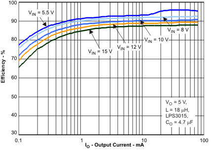 Figure 8. Efficiency vs Output Current IOUT (VOUT = 5 V)
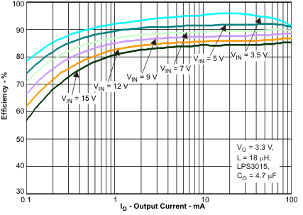 Figure 10. Efficiency vs Output Current IOUT (VOUT = 3.3 V)
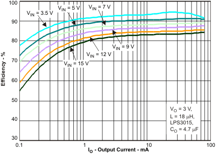 Figure 12. Efficiency vs Output Current IOUT (VOUT = 3 V)
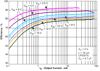 Figure 14. Efficiency vs Output Current IOUT (VOUT = 2 V)
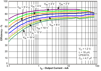 Figure 16. Efficiency vs Output Current IOUT (VOUT = 1.2 V)
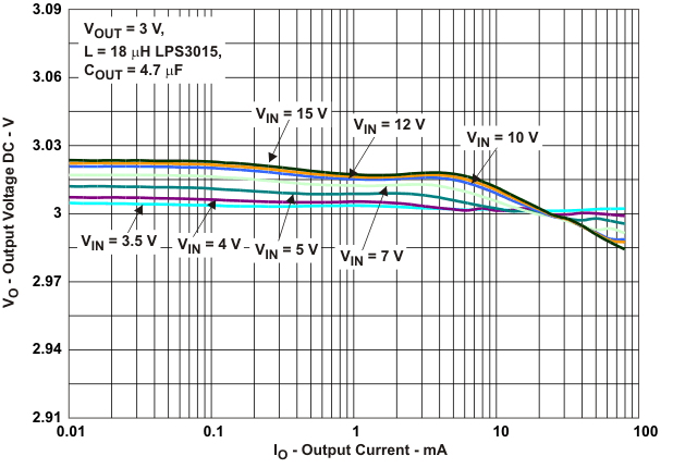 Figure 18. 3.0-V Output Voltage DC Regulation
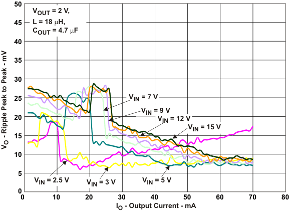 Figure 20. VOUT 2.0-V Output Ripple Voltage Peak to Peak
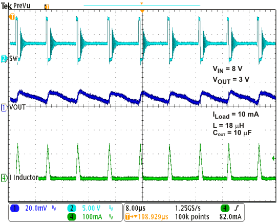
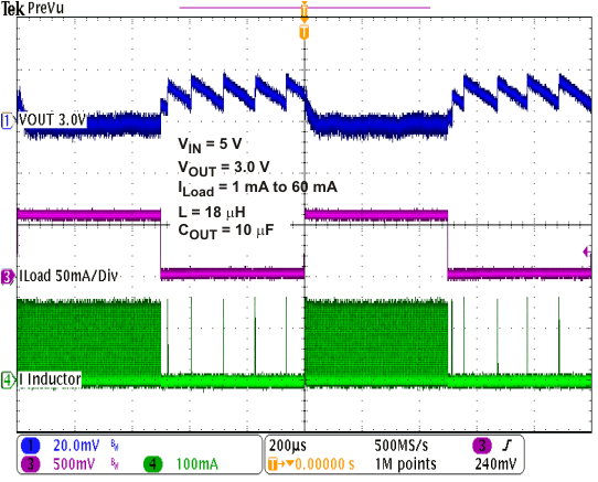 Figure 24. Load Transient Response for 3-V Output Voltage
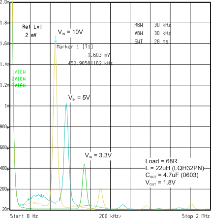 Figure 26. TPS62120 Spurious Output Noise
COUT = 4.7 µF
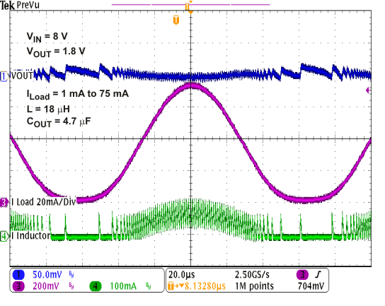 Figure 28. AC Load Regulation Performance for 1.8-V Output Voltage
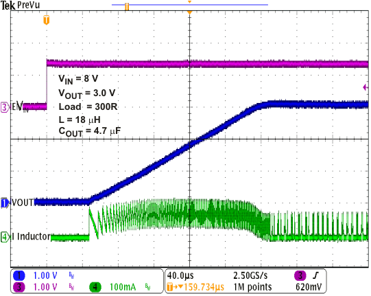 Figure 30. Startup VOUT = 3 V
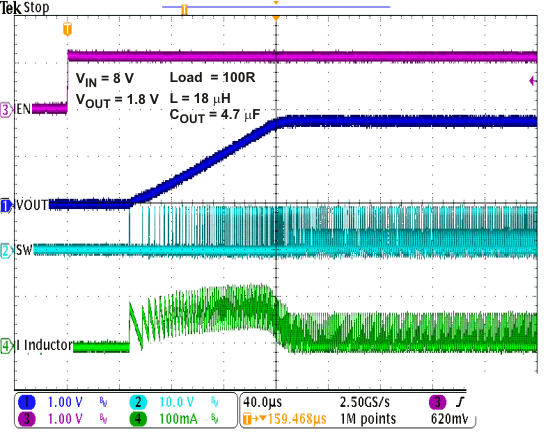 Figure 32. Startup VOUT 1.8 V
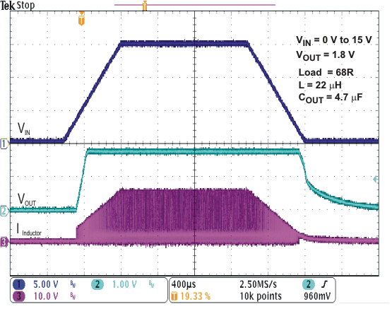 Figure 34. Input Voltage Ramp Up/Down
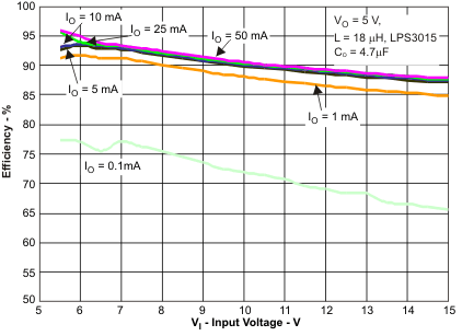 Figure 9. Efficiency vs Input Voltage VIN (VOUT = 5 V)
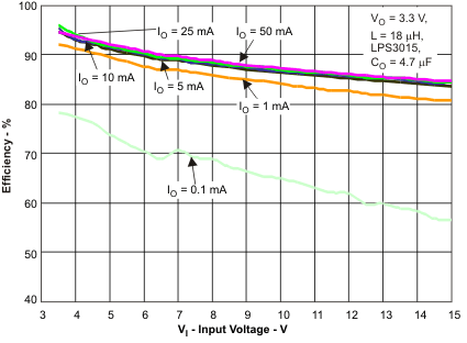 Figure 11. Efficiency vs Input Voltage VIN (VOUT = 3.3 V)
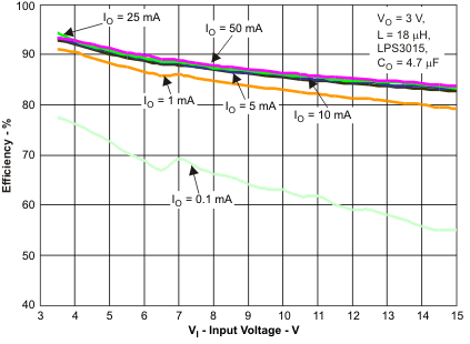 Figure 13. Efficiency vs Input Voltage VIN (VOUT = 3 V)
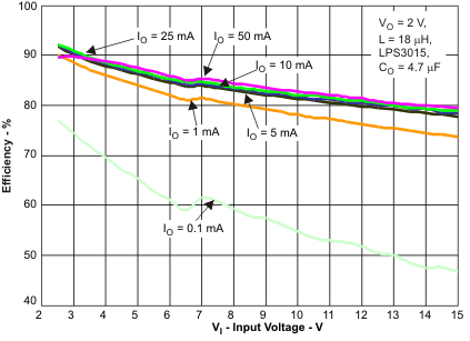 Figure 15. Efficiency vs Input Voltage VIN (VOUT = 2 V)
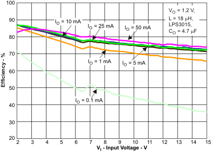 Figure 17. Efficiency vs Input Voltage VIN (VOUT = 1.2 V)
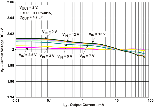 Figure 19. 2.0-V Output Voltage DC Regulation
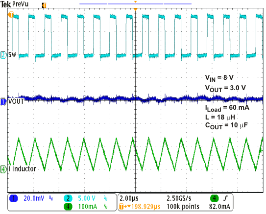 Figure 21. Typical Operation IOUT 60mA
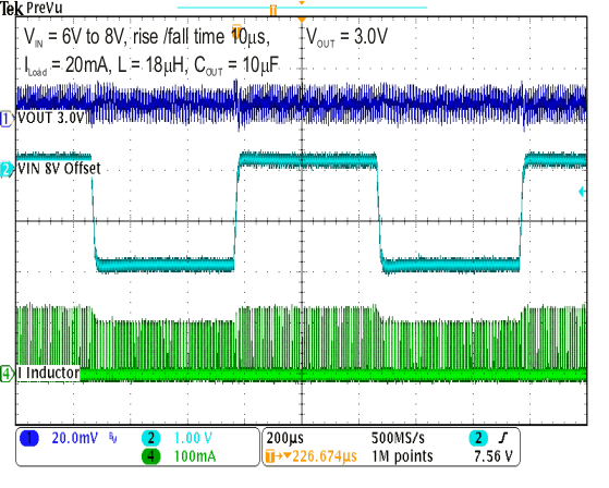 Figure 23. Line Transient Response for 3-V Output Voltage
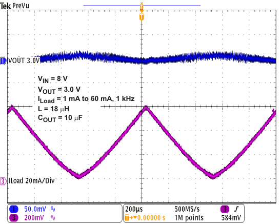 Figure 25. AC Load Regulation Performance for 3-V Output Voltage
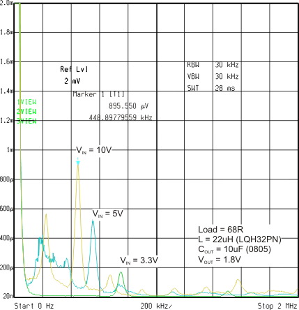 Figure 27. TPS62120 Spurious Output Noise
COUT = 10 µF
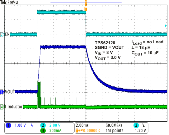 Figure 29. Output Discharge With SGND Pin Connected to VOUT
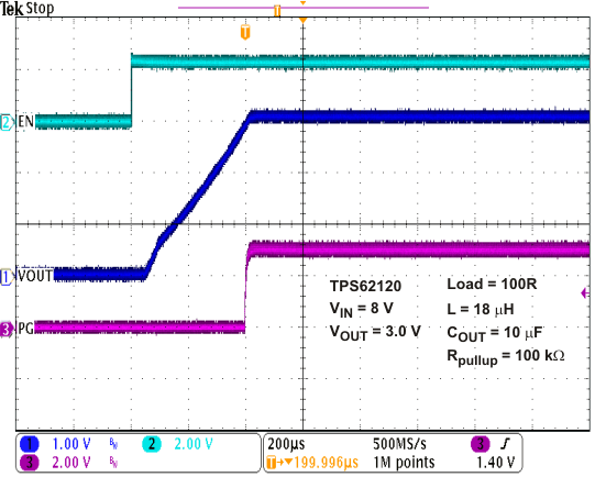 Figure 31. Power Good Output During Startup
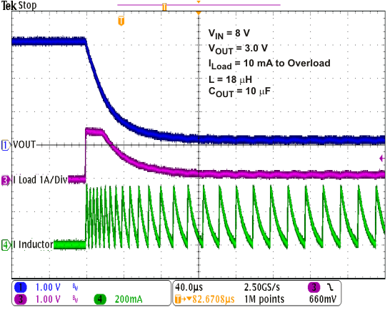 Figure 33. Output Overload Protection
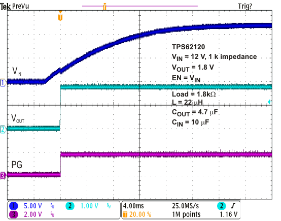 Figure 35. Startup From a High-Impedance Source
9.2.2 Standard Circuit for TPS62122
Beside the power good open drain output (PG pin) and the open drain output for output discharge (SGND pin) the TPS62122 provides the same functionality as the TPS62120.
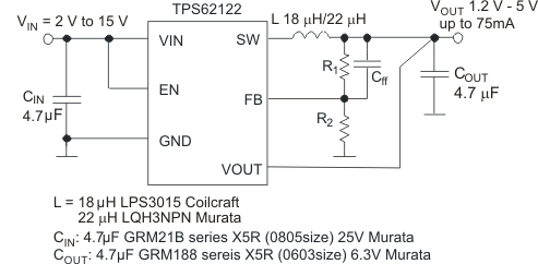 Figure 36. Standard Circuit for TPS62122
9.3 System Examples
The TPS6212x is operating with a wide input voltage range from 2 V to 15 V. An open-drain power good output and an additional SGND pin is available in the TPS62120 for output voltage regulation and to discharge the output capacitor.
9.3.1 TPS62120 1.8-V Output Voltage Configuration
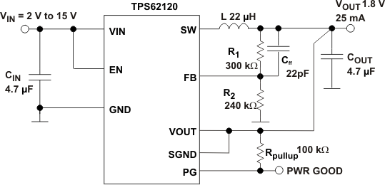 Figure 37. TPS62120 1.8-V Output Voltage Configuration
9.3.2 TPS62120 3.06-V Output Voltage Configuration
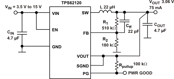 Figure 38. TPS62120 3.06-V Output Voltage Configuration
9.3.3 TPS62122 2.0-V Output Voltage Configuration
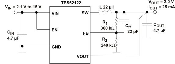 Figure 39. TPS62122 2.0-V Output Voltage Configuration
9.3.4 TPS62120 1.8-V VOUT Configuration Powered From a High-Impedance Source
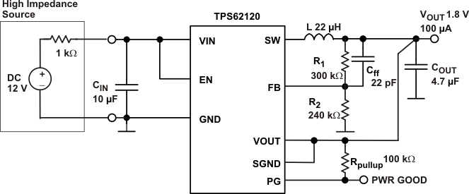 Figure 40. TPS62120 1.8-V VOUT Configuration Powered From a High-Impedance Source