SLVS916I July 2010 – October 2019 TPS63020 , TPS63021
PRODUCTION DATA.
- 1 Features
- 2 Applications
- 3 Description
- 4 Revision History
- 5 Pin Configuration and Functions
- 6 Specifications
- 7 Detailed Description
- 8 Application and Implementation
- 9 Power Supply Recommendations
- 10Layout
- 11Device and Documentation Support
- 12Mechanical, Packaging, and Orderable Information
Package Options
Mechanical Data (Package|Pins)
- DSJ|14
Thermal pad, mechanical data (Package|Pins)
- DSJ|14
Orderable Information
8.2.4 Application Curves
Table 4. Components for Application Characteristic Curves for VOUT = 3.3 V(1)(2)
| REFERENCE | DESCRIPTION | PART NUMBER | MANUFACTURER |
|---|---|---|---|
| U1 | High Efficiency Single Inductor Buck-Boost Converter With 4-A Switches | TPS63020 or TPS63021 | Texas Instruments |
| L1 | 1.5 μH, 4 mm x 4 mm x 2 mm | XFL4020-152ML | Coilcraft |
| C1 | 2 × 10 μF 6.3 V, 0603, X5R ceramic | GRM188R60J106ME84D | muRata |
| C2 | 3 × 22 μF 6.3 V, 0603, X5R ceramic | GRM188R60J226MEAOL | muRata |
| C3 | 0.1 μF, X5R or X7R ceramic | Standard | Standard |
| R1 | 1 MΩ at TPS63020, 0 Ω at TPS63021 | Standard | Standard |
| R2 | 180 kΩ at TPS63020, not used at TPS63021 | Standard | Standard |
| R3 | 1 MΩ | Standard | Standard |
(1) See Third-Party Products Discalimer.
(2) For other output voltages, refer to Table 3 for resistor values.
Table 5. Typical Characteristics Curves
| PARAMETER | CONDITIONS | FIGURE |
|---|---|---|
| EFFICIENCY | ||
| Efficiency vs Output Current, TPS63020 (Power save mode enabled) | VIN = 1.8 V, 2.4 V, 3.6 V, VOUT = 2.5 V, 4.5 V, PS/SYNC = Low | Figure 8 |
| Efficiency vs Output Current, TPS63020 (PWM only) | VIN = 1.8 V, 2.4 V, 3.6 V, VOUT = 2.5 V, 4.5 V, PS/SYNC = High | Figure 9 |
| Efficiency vs Output Current, TPS63021 (Power save mode enabled) | VIN = 2.4 V, 3.6 V, VOUT = 3.3 V, PS/SYNC = Low | Figure 10 |
| Efficiency vs Output Current, TPS63021 (PWM only) | VIN = 2.4 V, 3.6 V, VOUT = 3.3 V, PS/SYNC = High | Figure 11 |
| Efficiency vs Input Voltage, TPS63020 (Power save mode enabled) | VOUT = 2.5 V, Load = 10 mA, 500 mA, 1 A, 2 A, PS/SYNC = Low | Figure 12 |
| Efficiency vs Input Voltage, TPS63020 (Power save mode enabled) | VOUT = 4.5 V, Load = 10 mA, 500 mA, 1 A, 2 A, PS/SYNC = Low | Figure 13 |
| Efficiency vs Input Voltage, TPS63020 (PWM only) | VOUT = 2.5 V, Load = 10 mA, 500 mA, 1 A, 2 A, PS/SYNC = Low | Figure 14 |
| Efficiency vs Input Voltage, TPS63020 (PWM only) | VOUT = 2.5 V, Load = 10 mA, 500 mA, 1 A, 2 A, PS/SYNC = Low | Figure 15 |
| Efficiency vs Input Voltage, TPS63021 (Power save mode enabled) | VOUT = 3.3 V, Load = 10 mA, 500 mA, 1 A, 2 A, PS/SYNC = Low | Figure 16 |
| Efficiency vs Input Voltage, TPS63021 (PWM only) | VOUT = 3.3 V, Load = 10 mA, 500 mA, 1 A, 2 A, PS/SYNC = Low | Figure 17 |
| REGULATION ACCURACY | ||
| Load Regulation, PWM Boost Operation, TPS63020 | VIN = 3.6 V , VOUT = 4.5 V, PS/SYNC = High | Figure 18 |
| Load Regulation, PWM Buck Operation, TPS63020 | VIN = 3.6 V, VOUT = 2.5 V, PS/SYNC = High | Figure 19 |
| Load Regulation, PWM Operation, TPS63021 | VIN = 3.6 V, VOUT = 3.3 V, PS/SYNC = High | Figure 20 |
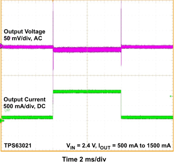
| Load Transient, TPS63021 | VIN = 2.4 V, VOUT = 3.3 V, Load = 500 mA to 1.5 A | Figure 21 |
| Load Transient, TPS63021 | VIN = 4.2 V, VOUT = 3.3 V, Load = 500 mA to 1.5 A | Figure 22 |
| Line Transient, TPS63021 | VIN = 3.0 V to 3.7 V, VOUT = 3.3 V, Load = 1.5 A | Figure 23 |
| START-UP | ||
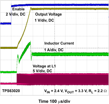
| Start-up Behavior from Rising Enable, TPS63021 | VIN = 2.4 V, VOUT = 3.3 V, Load = 2.2 Ω | Figure 24 |
| Start-up Behavior from Rising Enable, TPS63021 | VIN = 4.2 V, VOUT = 3.3 V, Load = 2.2 Ω | Figure 25 |
| Start-up Behavior from Rising Enable, TPS63021 | VIN = 2.4 V, VOUT = 3.3 V, Load = 2.2 Ω | Figure 26 |
| Start-up Behavior from Rising Enable, TPS63021 | VIN = 4.2 V, VOUT = 3.3 V, Load = 2.2 Ω | Figure 27 |
 Figure 8. Efficiency Versus Output Current, TPS63020, Power Save Enabled
  Figure 10. Efficiency Versus Output Current, TPS63021, Power Save Enabled
  Figure 12. Efficiency Versus Input Voltage, TPS63020, VOUT = 2.5 V, Power Save Enabled
  Figure 14. Efficiency Versus Input Voltage, TPS63020, VOUT = 2.5 V, Power Save Disabled
  Figure 16. Efficiency Versus Input Voltage, TPS63021, Power Save Enabled
  Figure 18. Output Voltage Versus Output Current, TPS63020, Power Save Disabled
  Figure 20. Output Voltage Versus Output Current, TPS63021, Power Save Disabled
  Figure 22. Load Transient Response, TPS63021
  Figure 9. Efficiency Versus Output Current, TPS63020, Power Save Disabled
  Figure 11. Efficiency Versus Output Current, TPS63021, Power Save Disabled
  Figure 13. Efficiency Versus Input Voltage, TPS63020, VOUT = 4.5 V, Power Save Enabled
  Figure 15. Efficiency Versus Input Voltage, TPS63020, VOUT = 4.5 V, Power Save Disabled
  Figure 17. Efficiency Versus Input Voltage, TPS63021, Power Save Disabled
  Figure 19. Output Voltage Versus Output Current, TPS63020, Power Save Enabled
  Figure 21. Load Transient Response, TPS63021
  Figure 23. Line Transient Response, TPS63021
  Figure 25. Start-up Behavior from Rising Enable, TPS63020
  Figure 27. Start-up Behavior from Rising Enable, TPS63020
