SLVS916I July   2010  – October 2019 TPS63020 , TPS63021

PRODUCTION DATA.  

  1. Features
  2. Applications
  3. Description
    1.     Device Images
      1.      Simplified Schematic
      2.      Efficiency vs Output Current
  4. Revision History
  5. Pin Configuration and Functions
    1.     Pin Functions
  6. Specifications
    1. 6.1 Absolute Maximum Ratings
    2. 6.2 ESD Ratings
    3. 6.3 Recommended Operating Conditions
    4. 6.4 Thermal Information
    5. 6.5 Electrical Characteristics
    6. 6.6 Typical Characteristics
  7. Detailed Description
    1. 7.1 Overview
    2. 7.2 Functional Block Diagram
    3. 7.3 Feature Description
      1. 7.3.1 Dynamic Voltage Positioning
      2. 7.3.2 Dynamic Current Limit
      3. 7.3.3 Device Enable
      4. 7.3.4 Power Good
      5. 7.3.5 Overvoltage Protection
      6. 7.3.6 Undervoltage Lockout
      7. 7.3.7 Overtemperature Protection
    4. 7.4 Device Functional Modes
      1. 7.4.1 Soft-start and Short Circuit Protection
      2. 7.4.2 Buck-Boost Operation
      3. 7.4.3 Control Loop
      4. 7.4.4 Power Save Mode and Synchronization
  8. Application and Implementation
    1. 8.1 Application Information
    2. 8.2 Typical Application
      1. 8.2.1 Design Requirements
      2. 8.2.2 Detailed Design Procedure
        1. 8.2.2.1 Custom Design with WEBENCH Tools
        2. 8.2.2.2 Inductor Selection
        3. 8.2.2.3 Output Capacitor Selection
        4. 8.2.2.4 Input Capacitor Selection
        5. 8.2.2.5 Bypass Capacitor
      3. 8.2.3 Setting The Output Voltage
      4. 8.2.4 Application Curves
    3. 8.3 System Examples
      1. 8.3.1 Improved Transient Response for 2 A Load Current
      2. 8.3.2 Supercapacitor Backup Power Supply With Active Cell Balancing
      3. 8.3.3 Low-Power TEC Driver
  9. Power Supply Recommendations
  10. 10Layout
    1. 10.1 Layout Guidelines
    2. 10.2 Layout Example
    3. 10.3 Thermal Considerations
  11. 11Device and Documentation Support
    1. 11.1 Receiving Notification of Documentation Updates
    2. 11.2 Device Support
      1. 11.2.1 Custom Design with WEBENCH Tools
      2. 11.2.2 Third-Party Products Disclaimer
    3. 11.3 Documentation Support
      1. 11.3.1 Related Documentation
    4. 11.4 Related Links
    5. 11.5 Support Resources
    6. 11.6 Trademarks
    7. 11.7 Electrostatic Discharge Caution
    8. 11.8 Glossary
  12. 12Mechanical, Packaging, and Orderable Information

Package Options

Mechanical Data (Package|Pins)
Thermal pad, mechanical data (Package|Pins)
Orderable Information

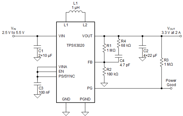
Improved Transient Response for 2 A Load Current

Capacitor C4 and resistor R4 are added for improved load transient performance.

TPS63020 TPS63021 schem-app-2A-slvs916.gifFigure 28. Application Circuit for 2 A Load Current