SLVSBB6F March 2012 – July 2015 TPS65300-Q1
PRODUCTION DATA.
- 1 Features
- 2 Applications
- 3 Description
- 4 Revision History
- 5 Pin Configuration and Functions
-
6 Specifications
- 6.1 Absolute Maximum Ratings
- 6.2 ESD Ratings
- 6.3 Recommended Operating Conditions
- 6.4 Thermal Information
- 6.5 DC Characteristics
- 6.6 Timing Requirements
- 6.7 Switching Characteristics
- 6.8 Typical Characteristics
- 6.9 5-V Linear Regulator (5VO)
- 6.10 3.3-V Linear Regulator Controller (3.3VO)
- 6.11 1.234-V Linear Regulator Controller (1.2VO)
- 7 Detailed Description
-
8 Application and Implementation
- 8.1 Application Information
- 8.2
Typical Application
- 8.2.1 Design Requirements
- 8.2.2 Detailed Design Procedure
- 8.2.3 Application Curves
- 9 Power Supply Recommendations
- 10Layout
- 11Device and Documentation Support
- 12Mechanical, Packaging, and Orderable Information
Package Options
Mechanical Data (Package|Pins)
Thermal pad, mechanical data (Package|Pins)
- PWP|24
Orderable Information
1 Features
- Qualified for Automotive Applications
- AEC-Q100 Qualified with the Following Results
- Device Temperature Grade 1: –40°C to 125°C Ambient Operating Temperature Range
- Device HBM ESD Classification Level H2
- Device CDM ESD Classification Level C4B
- Input VIN Range 5.6 V to 40 V, With Transients up to 45 V
- All Outputs Support Ceramic Output Capacitors for Stability
- Switch-Mode Regulator With Integrated High-Side Switch
- Recommended Switch-Mode Frequency Range 2 MHz to 3 MHz
- Overcurrent Protection and 1.2-A Peak Switch Current
- One Linear Regulators and Two Linear Regulator Controllers With 0.8-V ±1.5% Reference
- Status Indicator Output of IGN_EN Input
- Soft Start on Ignition (IGN_EN)/Enable Input (EN) Cycle
- External Clock Input for Synchronization
- Programmable Power-On-Reset Delay, Reset-Function Filter Timer for Fast Negative Transients
- Voltage Supervisor for the Following Supplies
- VREG, 3.3 V, 1.234 V
- Thermal Shutdown Protection for Excessive Power Dissipation
- Operating Junction Temperature Range: –40°C to 150°C
- Thermally Enhanced 24-Pin HTSSOP or 24-Pin VQFN Package
2 Applications
- Power Supply for TMS570 Microcontrollers
- Power Supply for C28XXX DSP
- General-Purpose Power Supply for Automotive Applications
- Microcontroller and DSP
3 Description
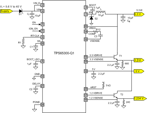
The TPS65300-Q1 power supply is a combination of a single switch-mode buck power supply and three linear regulators. This device is a monolithic high-voltage switching regulator with an integrated 1.2-A peak current switch, 45-V power MOSFET, and one low-voltage linear regulator and two voltage-regulator controllers.
The device has a voltage supervisor which monitors the output of the switch-mode power supply, the
3.3-V linear regulator, and the 1.234-V linear regulator. An external timing capacitor is used to set the power-on delay and the release of the reset output nRST. This reset output is also used to indicate if the switch-mode supply, the 3.3-V linear regulator supply, or the 1.234-V linear regulator supply is outside the set limits. The 5-V regulator tracks the 3.3-V linear regulator within the specified limits.
The TPS65300-Q1 device has a switching frequency range from 2 MHz to 3 MHz, allowing the use of low-profile inductors and low-value input and output ceramic capacitors. External loop compensation gives the user the flexibility to optimize the converter response for the appropriate operating conditions.
This device has built-in protection features such as soft start on IGN_EN ON or enables cycle, pulse-by-pulse current-limit, thermal sensing, and shutdown because of excessive power dissipation.
Device Information
| PART NUMBER | PACKAGE | BODY SIZE (NOM) |
|---|---|---|
| TPS65300-Q1 | HTSSOP (24) | 7.80 mm × 4.40 mm |
| VQFN (24) | 5.00 mm × 4.00 mm |
Typical Application Schematic

4 Revision History
Changes from E Revision (March 2014) to F Revision
- Changed the word terminal back to pin throughout the document Go
- Changed the MIN, TYP, and MAX values for the 1.2VSENSE output voltage in the Electrical Characteristics table Go
- Changed the y-axis intervals for the 1.2VSENSE vs Temperature graphGo
Changes from D Revision (August 2013) to E Revision
- Added the Device Information table and the following new sections: Power Supply Recommendations, Device and Documentation Support, and Mechanical, Packaging, and Orderable InformationGo
- Changed the word pin to terminal throughout the document Go
- Moved the Pin Functions section into the Pin Configuration and Functions sectionGo
- Changed DC CHARACTERISTICS condition statement from TJ = –40°C to 150°C to TJ-Max = 150°CGo
- Changed min value for VIL of IGN_EN from 2 to 2.2 in the DC CHARACTERISTICS tableGo
- Moved all timing requirements out of the Electrical Characteristics table and into the Timing Requirements table Go
- Combined the general application equations with the practical equations to streamline the Typical Application section Go
- Changed Y-axis name from Current (mA) to Efficiency in Figure 17Go
- Moved the Efficiency vs Output Current on VREG graph and the scope plots from the Typical Characteristics section to the Application Curves section Go
Changes from C Revision (April 2013) to D Revision
- Changed VIH max limit from 4 to 3.6 V in DC Characteristics tableGo
- Added 3.7 V condition and values to Input High IIH parameter in DC Characteristics tableGo
- Changed ICharge unit from V to µA in DC Characteristics tableGo
- Changed internal resistor limit text in Ignition Enable Input, IGN_EN pin descriptionGo