SLVSDW6C April 2017 – April 2021 TPS7H1101A-SP
PRODUCTION DATA
- 1 Features
- 2 Applications
- 3 Description
- 4 Revision History
- 5 Pin Configuration and Functions
- 6 Specifications
- 7 Detailed Description
- 8 Application and Implementation
- 9 Power Supply Recommendations
- 10Layout
- 11Device and Documentation Support
- 12Mechanical, Packaging, and Orderable Information
Package Options
Mechanical Data (Package|Pins)
- HKR|16
- KGD|0
Thermal pad, mechanical data (Package|Pins)
Orderable Information
8.2.1.7 Compensation
Figure 8-13 shows a generic block diagram for TPS7H1101A-SP LDO with external compensation components. LDO incorporates nested loops, thus providing the high gain necessary to meet design performance.
 Figure 8-13 TPS7H1101A-SP Compensation
Resistor divider composed of Rtop and Rbottom determine the output voltage set points as indicated by Equation 2.
Output capacitor COUT introduces a pole and a zero as shown in the following.
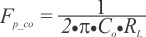
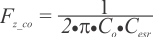
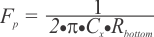
The TPS7H1101A-SP was designed so that the ESR of the output capacitor will not have a strong influence on the response of the LDO. However, an optional capacitor, Cx, can be added in parallel with the bottom feedback resistor to introduce a pole to cancel Fz_co. Equation 8 shows how to calculate the location of the pole introduced by Cx. To cancel the zero directly, Fp should be equal to Fz_co.
Cx is calculated to be 1000 pF for Co = 220 µF, Cesr = 45 mΩ, and Rbottom = 10 kΩ.
Figure 8-13 also includes a place holder for a feed forward capacitance Cff. Use of feed forward compensation can be more advantageous than use of Cx. Please reference application note Pros and Cons of Using a Feedforward Capacitor with a Low-Dropout Regulator for additional information on usage of CFF.
Internal compensation in the LDO cancels the output capacitor pole introduced by COUT and RL.
Ccomp introduces a dominant pole at low frequency. TI recommends that a Ccomp value of 10 nF.