SLVSFT8F February 2023 – December 2023 TPS7H1111-SEP , TPS7H1111-SP
PRODUCTION DATA
- 1
- 1 Features
- 2 Applications
- 3 Description
- 4 Device Options Table
- 5 Pin Configuration and Functions
- 6 Specifications
- 7 Parameter Measurement Information
-
8 Detailed Description
- 8.1 Overview
- 8.2 Functional Block Diagram
- 8.3 Feature Description
- 8.4 Device Functional Modes
-
9 Application and Implementation
- 9.1 Application Information
- 9.2 Typical Applications
- 9.3 Capacitors Tested
- 9.4 TID Effects
- 9.5 Power Supply Recommendations
- 9.6 Layout
- 10Device and Documentation Support
- 11Revision History
- 12Mechanical, Packaging, and Orderable Information
Package Options
Refer to the PDF data sheet for device specific package drawings
Mechanical Data (Package|Pins)
- PWP|28
Thermal pad, mechanical data (Package|Pins)
- PWP|28
Orderable Information
8.3.5 Soft Start and Noise Reduction
In addition to setting the output voltage, the SS_SET pin serves two other important functions: programming the soft start time and creating a noise filter for the internal reference current. In most applications, at least a 4.7 μF capacitor is recommended in order to obtain sufficient low noise performance. Larger value capacitors may be acceptable; however, there are diminishing returns in reduced output noise in capacitor values larger than 4.7μF.
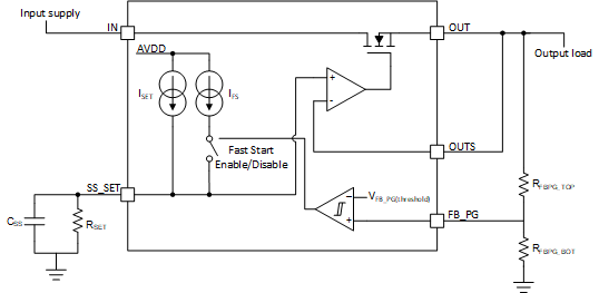
This capacitor also slows down the SS_SET voltage ramp rate, and therefore controls the LDO turn-on time (soft start). However, if the capacitor was only charged by the ISET current (nominally 100 μA), the startup time would be excessive. Therefore, there is an additional fast charge current source (IFS ≈ 2 mA) that is active during startup. Consequently, a 4.7μF capacitor will result in a nominal 3.7 ms soft start time. A simplified diagram of this circuitry is shown in Figure 8-3.
 Figure 8-3 Simplified Schematic Showing
Startup Circuitry
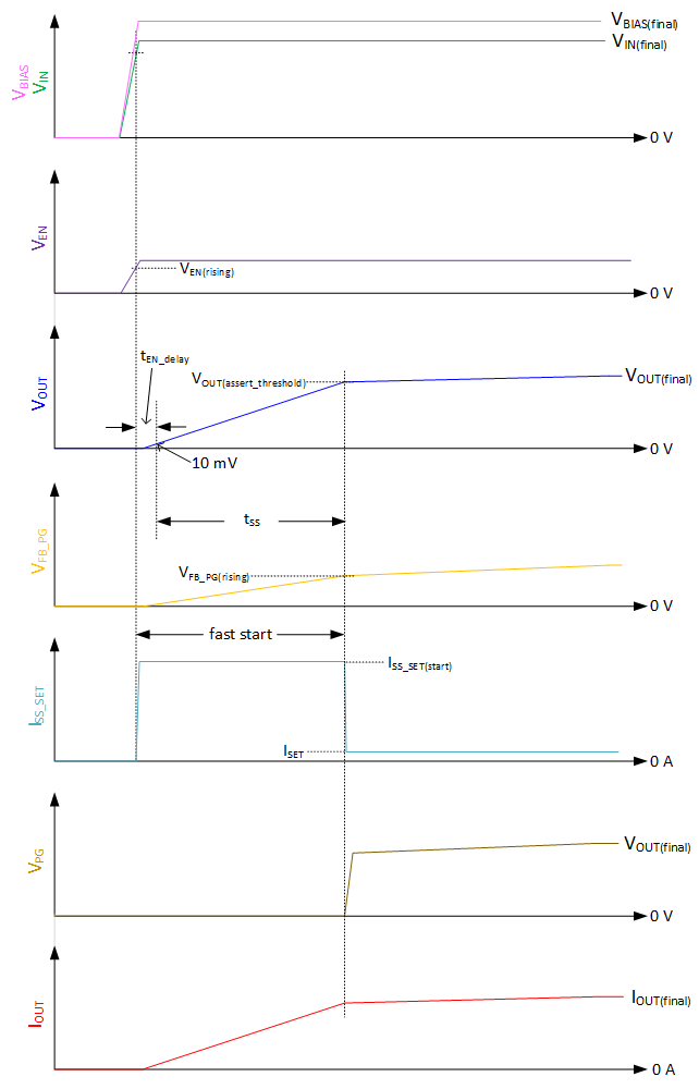
 This fast charge circuitry is active until the FB_PG threshold is reached (typically 300 mV). After the FB_PG threshold has been reached, the fast start current will turn off and the soft start time as shown in Equation 6 will be completed. CSS will continue charging to its final value (as determined by the RSET resistor) with the 100 μA (typ) reference current. An example startup waveform is shown in Figure 8-4. In this waveform it is assumed EN is fed a divided down version of VIN.
where
- tSS = soft start time
- ISS_SET(startup) = IFS + ISET = 2.1 mA (typ)
- V(assert_threshold) = configured value of VOUT for which PG is asserted (typically 90% of VOUT(final), see Section 8.3.6)
Note that the fast charge current (IFS) and set current (ISET) are both active during the soft start time (tSS) and are reported as ISS_SET(start) in the Electrical Characteristics table. This 2.1 mA typical value is valid for a 12 kΩ RREF resistor. As the fast charge current is internally derived from the current through the RREF resistor, values greater than or less than 12 kΩ will cause a decrease or increase of the IFS current respectively.
If the fast start circuitry is not desired, connect the FB_PG pin to VOUT. This will ensure the fast start circuitry is quickly turned-off as the FB_PG threshold is quickly reached. Note that this effects the PG pin behavior as well as described in Section 8.3.6.
 Figure 8-4 Simplified Schematic Showing
Startup Waveforms