JAJSOX0B March 2024 – November 2024 ADS127L18
PRODMIX
- 1
- 1 特長
- 2 アプリケーション
- 3 概要
- 4 Pin Configuration and Functions
- 5 Specifications
-
6 Parameter Measurement Information
- 6.1 Offset Error Measurement
- 6.2 Offset Drift Measurement
- 6.3 Gain Error Measurement
- 6.4 Gain Drift Measurement
- 6.5 NMRR Measurement
- 6.6 CMRR Measurement
- 6.7 PSRR Measurement
- 6.8 SNR Measurement
- 6.9 INL Error Measurement
- 6.10 THD Measurement
- 6.11 IMD Measurement
- 6.12 SFDR Measurement
- 6.13 Noise Performance
-
7 Detailed Description
- 7.1 Overview
- 7.2 Functional Block Diagram
- 7.3 Feature Description
- 7.4 Device Functional Modes
- 7.5 Programming
- 8 Register Map
- 9 Application and Implementation
- 10Device and Documentation Support
- 11Revision History
- 12Mechanical, Packaging, and Orderable Information
7.3.1 Analog Inputs (AINP, AINN)
The analog inputs of the ADC channels are differential, with the input defined as a difference voltage: VIN = VAINP – VAINN. For best performance, drive the input with a differential signal with the common-mode voltage centered to mid-supply (AVDD1 + AVSS) / 2. Tie unused inputs to ground or a dc voltage within the AVSS to AVDD1 power supply range.
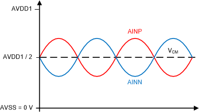
The ADC accepts either unipolar or bipolar input signals by configuring the AVDD1 and AVSS power supplies accordingly. Figure 7-1 illustrates an example of a differential signal in unipolar supply configuration. Symmetric input voltage headroom is provided when the common-mode voltage is equal to mid-supply (AVDD1 / 2). For unipolar operation, use AVDD1 = 5V and AVSS = 0V (mid- and low-speed modes offer the option of reduced AVDD1 supply voltage). The VCM pin provides a buffered common-mode voltage to level-shift the signal voltage in the external driver stage.
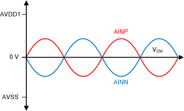
Figure 7-2 illustrates an example of a differential signal in bipolar supply configuration. The common-mode voltage of the signal is normally 0V. For bipolar operation, use AVDD1 and AVSS = ±2.5V (mid- and low-speed modes offer the option of reduced AVDD1 – AVSS supply voltage).
 Figure 7-1 Unipolar Differential
Input Signal
 Figure 7-2 Bipolar Differential Input
Signal
Figure 7-2 Bipolar Differential Input
SignalIn both bipolar and unipolar configurations, the ADC accepts single-ended input signals by tying the AINN input to AVSS, ground, or to mid-supply. However, because AINN is a fixed voltage, the full differential input swing range is not obtained. Thus, the ADC dynamic range is limited to the voltage swing of the AINP input (±2.5V or 0V to 5V for a 5V supply).
The circuit of Figure 7-3 shows the simplified analog input circuit of the ADC channels. Diodes protect the analog inputs from electrostatic discharge (ESD) events that occur during the manufacturing process and during printed circuit board (PCB) assembly when manufactured in an ESD-controlled environment. If the inputs are driven below AVSS – 0.3 V, or above AVDD1 + 0.3 V, the protection diodes potentially conduct. If these conditions are possible, use external clamp diodes, series resistors, or both to limit the input current to the value shown in the Absolute Maximum Ratings section.
 Figure 7-3 Analog Input Circuit
The input multiplexers of the ADC channels are independently configurable. The multiplexer offers the option of normal or reverse signal polarities and internal test modes. The test modes are used for ADC performance testing and diagnostics. The input-short test mode verifies noise and offset errors by shorting the inputs to mid-supply voltage. Full-scale range is tested by selecting the +FS or –FS connection. To avoid clipped output codes during evaluation, reduce the value of the gain registers or program the ADC to the extended range mode. The CMRR test mode verifies CMRR performance by shorting the inputs together and the user applying a dc or ac test signal to the AINPn or AINNn input. The resulting data is analyzed by the user to determines CMRR performance. Enable the input precharge buffers for best accuracy when using the test modes.
Table 7-1 shows the switch configurations of the input multiplexer circuit of Figure 7-3.
| CHn_MUX[2:0] BITS | CLOSED SWITCHES | DESCRIPTION |
|---|---|---|
| 000b | S1, S4 | Normal polarity input |
| 001b | S2, S3 | Reverse polarity input |
| 010b | S9, S10 | Input short for offset voltage and noise test |
| 011b | S1, S10 | Input short with user applied signal to AINPn for CMRR test |
| 100b | S4, S10 | Input short with user applied signal to AINNn for CMRR test |
| 101b | S6, S7 | –FS dc signal for gain test |
| 110b | S5, S8 | +FS dc signal for gain test |
| 111b | S5, S8 | +FS dc signal for gain test |
The input sampling capacitor CIN is part of the simplified input sampling network denoted in the dashed box of Figure 7-3. The instantaneous charge demand of CIN requires the signal to settle within a half cycle of the modulator frequency t = 1 / (2 · fMOD). To satisfy this requirement, the driver bandwidth is typically much larger than the original signal frequency. The bandwidth of the driver is determined as sufficient when the THD and SNR data sheet performance are achieved. Because the modulator sampling rate is eight times slower in low-speed mode compared to high-speed mode, more time is available for driver settling.
The charge required by the input sampling capacitor is modeled as an average input current of the ADC inputs. As shown in Equation 22 and Equation 16, the input current is comprised of differential and absolute components.
where:
- fMOD = fCLK / 2
- CIN = 7.4pF (1x input range), 3.6pF (2x input range)
where:
- fMOD = fCLK / 2
- CCM = 0.35pF (1x input range), 0.17pF (2x input range)
For fMOD = 12.8MHz (high-speed mode), CIN = 7.4pF and CCM = 0.3pF, the input current resulting from the differential voltage is 95μA/V and the input current resulting from the absolute voltage is 4.5μA/V. For example, if AINPn = 4.5V and AINNn = 0.5 , then VIN = 4V. The total AINPn input current = (4V · 95μA/V) + (4.5V · 4.5μA/V) = 400μA. The total AINNn current is (–4V · 95μA/V) + (0.5 · 4.5μA/V) = –378μA.
The device incorporates input precharge buffers to significantly reduce the charge required by capacitor CIN. In operation, the precharge buffers provide the charging current. Near the end of the sampling phase, capacitor CIN is nearly fully charged. The buffers are disconnected (S11 and S12 of Figure 7-3 in up positions) to allow the external driver to provide the fine charge to the capacitor. When the sample phase is completed, the sampling capacitor is discharged to complete the cycle, at which time the sample process repeats. The operation of the precharge buffers reduces the input current by more than 99%, and in many cases leads to improved THD and SNR performance. The precharge buffers are enabled by the CHn_BUFP and CHn_BUFN bits of the CHn_CFG1 register. If the AINN input of any channel is tied to ground or to a low-impedance source, disable the AINN buffer to reduce power consumption. A single-ended input application is an example of a low-impedance source.