JAJSEC1C November 2019 – July 2020 ADS8686S
PRODUCTION DATA
- 1 特長
- 2 アプリケーション
- 3 概要
- 4 Revision History
- 5 Pin Configuration and Functions
-
6 Specifications
- 6.1 Absolute Maximum Ratings
- 6.2 ESD Ratings
- 6.3 Recommended Operating Conditions
- 6.4 Thermal Information
- 6.5 Electrical Characteristics
- 6.6 Timing Requirements
- 6.7 Switching Characteristics
- 6.8 Timing Diagrams: Universal
- 6.9 Timing Diagrams: Parallel Data Read
- 6.10 Timing Diagrams: Serial Data Read
- 6.11 Typical Characteristics
-
7 Detailed Description
- 7.1 Overview
- 7.2 Functional Block Diagram
- 7.3 Feature Description
- 7.4
Device Functional Modes
- 7.4.1
Device Interface: Pin Description
- 7.4.1.1 REFSEL (Input)
- 7.4.1.2 RESET (Input)
- 7.4.1.3 SEQEN (Input)
- 7.4.1.4 HW_RANGESEL[1:0] (Input)
- 7.4.1.5 SER/BYTE/PAR (Input)
- 7.4.1.6 DB[3:0] (Input/Output)
- 7.4.1.7 DB4/SER1W (Input/Output)
- 7.4.1.8 DB5/CRCEN (Input/Output)
- 7.4.1.9 DB[7:6] (Input/Output)
- 7.4.1.10 DB8 (Input/Output)
- 7.4.1.11 DB9/BYTESEL (Input/Output)
- 7.4.1.12 DB10/SDI (Input/Output)
- 7.4.1.13 DB11/SDOB (Input/Output)
- 7.4.1.14 DB12/SDOA (Input/Output)
- 7.4.1.15 DB13/OS0 (Input/Output)
- 7.4.1.16 DB14/OS1 (Input/Output)
- 7.4.1.17 DB15/OS2 (Input/Output)
- 7.4.1.18 WR/BURST (Input)
- 7.4.1.19 SCLK/RD (Input)
- 7.4.1.20 CS (Input)
- 7.4.1.21 CHSEL[2:0] (Input)
- 7.4.1.22 BUSY (Output)
- 7.4.1.23 CONVST (Input)
- 7.4.2 Device Modes of Operation
- 7.4.1
Device Interface: Pin Description
- 7.5 Programming
- 7.6 Register Maps
- 8 Application and Implementation
- 9 Power Supply Recommendations
- 10Layout
- 11Device and Documentation Support
7.4.2.3 Reset Functionality
The ADS8686S supports two reset modes: full and partial. The reset mode selected is dependent on the length of the reset low pulse.
A partial reset is applied when the RESET pin is held low between 40 ns and 500 ns. A partial reset reinitializes the sequencer, digital filter, SPI, and SAR ADC modules.
The ongoing conversion result is discarded on completion of a partial reset. The partial reset does not affect the register values programmed in software mode or the user configuration latched in hardware and software modes. In software mode, a dummy conversion is required after a partial reset.
After the release of a partial reset, the device is fully functional after 50 ns and a dummy conversion can be initiated.
A full reset is applied when the RESET pin is held low for a minimum of 1.2 µs. A full reset configures the device to its default power-on state. Hardware or software mode, the internal or external reference, and the type of interface are configured when the ADS8686S is released from a full reset.
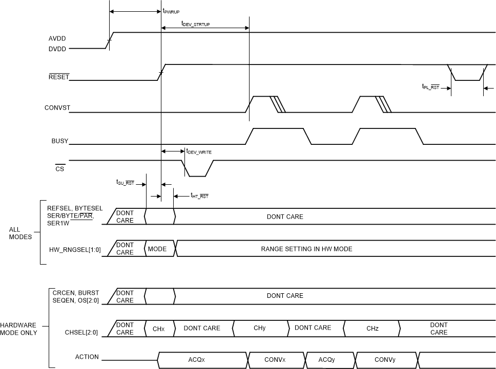
At power-up, the RESET signal must be kept low until the AVDD and DVDD supplies are stable. The RESET signal can be released after the supplies ramp to stable operating conditions. The logic level of the HW_RNGSELx, REFSEL, SER/BYTE/ PAR, DB9/BYTESEL, and DB4/ SER1W pins are latched when the RESET pin is released to determine the device configuration.
After 15 ms from releasing RESET, the device is completely reconfigured and a conversion can be initiated.
In hardware mode, the DB8CRCEN, OSx, BURST, and SEQEN pin status is also latched when the RESET pin transitions from low to high in full reset mode. The changes to these signals are ignored after they are latched until the next full reset. In hardware mode, the analog input range (HW_RNGSELx signals) can be configured during either a full or a partial reset or during normal operation, but hardware or software mode selection requires a full reset to reconfigure when this setting is latched.
In hardware mode, the CHSELx and HW_RNGSELx pins are monitored at release from both a full and a partial reset to perform the following actions:
- Select the first analog input channel pair to acquire for conversion
- Configure the sequencer
- Select the analog input voltage range
The CHSELx signals are not latched at reset. The channel pair selected for next conversion, or the hardware sequencer, can be reconfigured during normal operation by setting and maintaining the CHSELx signal level before the CONVST rising edge, and holding the signal state constant until BUSY is held high by the device. See the Section 7.4.2.4 section for further details.
The HW_RNGSELx signals are not latched in hardware mode. A logic change on these pins has an immediate effect on the range selected. See the Section 7.3.4 section for additional details.
In software mode, all device functionality is configured by controlling the on-chip registers. Figure 7-11 shows the device reset configuration and Table 7-6 lists an overview of the pin functionality.
 Figure 7-11 ADS8686S Configuration at Reset