SLVSCV5E March   2015  – December 2024 ATL431 , ATL432

PRODUCTION DATA  

  1.   1
  2. Features
  3. Applications
  4. Description
  5. Pin Configuration and Functions
  6. Specifications
    1. 5.1 Absolute Maximum Ratings
    2. 5.2 ESD Ratings
    3. 5.3 Recommended Operating Conditions
    4. 5.4 Thermal Information
    5. 5.5 Electrical Characteristics, ATL431Ax, ATL432Ax
    6. 5.6 Electrical Characteristics, ATL431Bx, ATL432Bx
    7. 5.7 Typical Characteristics
  7. Parameter Measurement Information
  8. Detailed Description
    1. 7.1 Overview
    2. 7.2 Functional Block Diagram
    3. 7.3 Feature Description
    4. 7.4 Device Functional Modes
      1. 7.4.1 Open Loop (Comparator)
      2. 7.4.2 Closed Loop
  9. Application and Implementation
    1. 8.1 Application Information
    2. 8.2 Typical Applications
      1. 8.2.1 Comparator With Integrated Reference (Open-Loop)
        1. 8.2.1.1 Design Requirements
        2. 8.2.1.2 Detailed Design Procedure
          1. 8.2.1.2.1 Basic Operation
          2. 8.2.1.2.2 Overdrive
          3. 8.2.1.2.3 Output Voltage and Logic Input Level
            1. 8.2.1.2.3.1 Input Resistance
        3. 8.2.1.3 Application Curve
      2. 8.2.2 Shunt Regulator/Reference
        1. 8.2.2.1 Design Requirements
        2. 8.2.2.2 Detailed Design Procedure
          1. 8.2.2.2.1 Programming Output/Cathode Voltage
          2. 8.2.2.2.2 Total Accuracy
          3. 8.2.2.2.3 Stability
        3. 8.2.2.3 Application Curves
  10. Power Supply Recommendations
  11. 10Layout
    1. 10.1 Layout Guidelines
    2. 10.2 Layout Example
  12. 11Device and Documentation Support
    1. 11.1 Receiving Notification of Documentation Updates
    2. 11.2 Support Resources
    3. 11.3 Trademarks
    4. 11.4 Electrostatic Discharge Caution
    5. 11.5 Glossary
  13. 12Revision History
  14. 13Mechanical, Packaging, and Orderable Information

パッケージ・オプション

メカニカル・データ(パッケージ|ピン)
サーマルパッド・メカニカル・データ
発注情報

Parameter Measurement Information

The deviation parameters Vref(dev) and Iref(dev) are defined as the differences between the maximum and minimum values obtained over the rated temperature range. The average full-range temperature coefficient of the reference input voltage αVref is defined as:

ATL431 ATL432

αVref is positive or negative, depending on whether minimum Vref or maximum Vref, respectively, occurs at the lower temperature.

The dynamic impedance is defined as: ATL431 ATL432

When the device is operating with two external resistors (see Figure 6-2), the total dynamic impedance of the circuit is given by: ATL431 ATL432 which is approximately equal to ATL431 ATL432

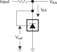
ATL431 ATL432 Test Circuit for VKA = VrefFigure 6-1 Test Circuit for VKA = Vref
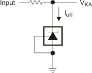
ATL431 ATL432 Test Circuit for Ioff
Figure 6-3 Test Circuit for Ioff
ATL431 ATL432 Test Circuit for Reference Impedance (ZKA)
Figure 6-5 Test Circuit for Reference Impedance (ZKA)
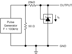
ATL431 ATL432 Test Circuit for Pulse ResponseFigure 6-7 Test Circuit for Pulse Response
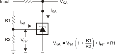
ATL431 ATL432 Test Circuit for VKA > VrefFigure 6-2 Test Circuit for VKA > Vref
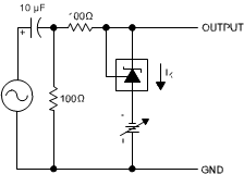
ATL431 ATL432 Test Circuit for Phase and Gain Measurement
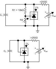
Figure 6-4 Test Circuit for Phase and Gain Measurement
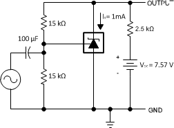
ATL431 ATL432 Test Circuit for Stability Boundary ConditionsFigure 6-6 Test Circuit for Stability Boundary Conditions