JAJS245G August   2007  – January 2024 CDCE949 , CDCEL949

PRODUCTION DATA  

  1.   1
  2. 特長
  3. アプリケーション
  4. 概要
  5. Pin Configuration and Functions
  6. Specifications
    1. 5.1 Absolute Maximum Ratings
    2. 5.2 ESD Ratings
    3. 5.3 Recommended Operating Conditions
    4. 5.4 Thermal Information
    5. 5.5 Electrical Characteristics
    6. 5.6 EEPROM Specification
    7. 5.7 Timing Requirements: CLK_IN
    8. 5.8 Timing Requirements: SDA/SCL
    9. 5.9 Typical Characteristics
  7. Parameter Measurement Information
  8. Detailed Description
    1. 7.1 Overview
    2. 7.2 Functional Block Diagram
    3. 7.3 Feature Description
      1. 7.3.1 Control Terminal Setting
      2. 7.3.2 Default Device Setting
      3. 7.3.3 SDA/SCL Serial Interface
      4. 7.3.4 Data Protocol
    4. 7.4 Device Functional Modes
      1. 7.4.1 SDA/SCL Hardware Interface
    5. 7.5 Programming
  9. Application and Implementation
    1. 8.1 Application Information
    2. 8.2 Typical Application
      1. 8.2.1 Design Requirements
      2. 8.2.2 Detailed Design Procedure
        1. 8.2.2.1 Spread Spectrum Clock (SSC)
        2. 8.2.2.2 PLL Frequency Planning
        3. 8.2.2.3 Crystal Oscillator Start-Up
        4. 8.2.2.4 Frequency Adjustment With Crystal Oscillator Pulling
        5. 8.2.2.5 Unused Inputs and Outputs
        6. 8.2.2.6 Switching Between XO and VCXO Mode
      3. 8.2.3 Application Curves
    3. 8.3 Power Supply Recommendations
    4. 8.4 Layout
      1. 8.4.1 Layout Guidelines
      2. 8.4.2 Layout Example
  10. Register Maps
    1. 9.1 SDA/SCL Configuration Registers
  11. 10Device and Documentation Support
    1. 10.1 Device Support
      1. 10.1.1 Development Support
    2. 10.2 Related Documentation
    3. 10.3 Related Links
    4. 10.4 ドキュメントの更新通知を受け取る方法
    5. 10.5 サポート・リソース
    6. 10.6 Trademarks
    7. 10.7 静電気放電に関する注意事項
    8. 10.8 用語集
  12. 11Revision History
  13. 12Mechanical, Packaging, and Orderable Information

パッケージ・オプション

メカニカル・データ(パッケージ|ピン)
サーマルパッド・メカニカル・データ
発注情報

Application Curves

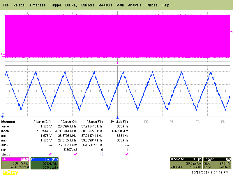
Figure 8-6, Figure 8-7, Figure 8-8, and Figure 8-9 show CDCEx949 measurements with the SSC feature enabled. Device configuration: 27-MHz input, 27-MHz output.

GUID-B9ED03B1-1D03-4250-840E-7D5AFF5FA329-low.pngFigure 8-6 fOUT = 27 MHz, VCO Frequency < 125 MHz, SSC (2% Center)
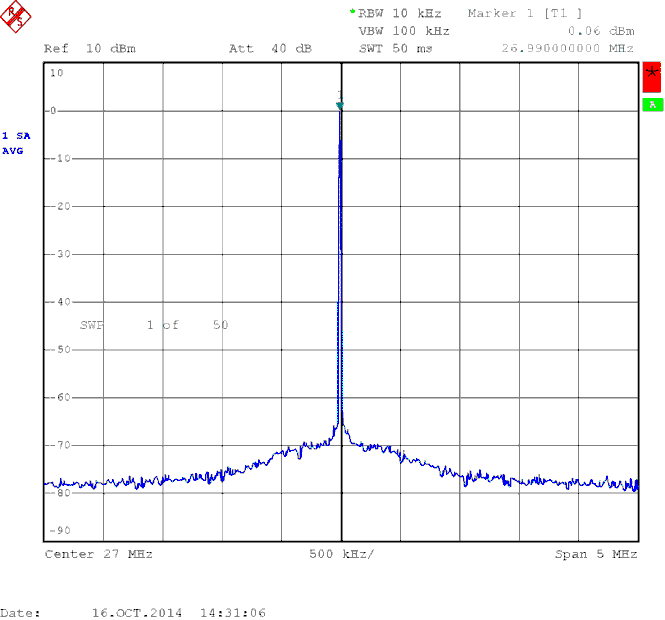
GUID-80FA0918-5C59-4F1B-8775-D2CEE5BEB349-low.pngFigure 8-8 Output Spectrum With SSC Off
GUID-A5BDC4CB-2F0A-405A-B2F8-FC971E57A599-low.pngFigure 8-7 fOUT = 27 MHz, VCO Frequency > 175 MHz, SSC (1%, Center)
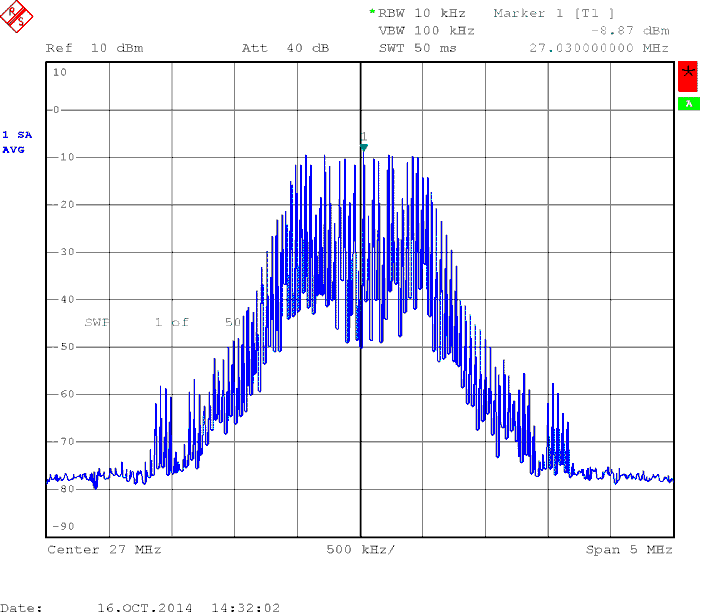
GUID-79C57B7D-451F-448B-918B-89954B45C445-low.pngFigure 8-9 Output Spectrum With SSC On, 2% Center