JAJSLD4B august 2020 – july 2023 DLP471TP
PRODUCTION DATA
- 1
- 1 特長
- 2 アプリケーション
- 3 概要
- 4 Revision History
- 5 Pin Configuration and Functions
-
6 Specifications
- 6.1 Absolute Maximum Ratings
- 6.2 Storage Conditions
- 6.3 ESD Ratings
- 6.4 Recommended Operating Conditions
- 6.5 Thermal Information
- 6.6 Electrical Characteristics
- 6.7 Switching Characteristics
- 6.8 Timing Requirements
- 6.9 System Mounting Interface Loads
- 6.10 Micromirror Array Physical Characteristics
- 6.11 Micromirror Array Optical Characteristics
- 6.12 Window Characteristics
- 6.13 Chipset Component Usage Specification
- 7 Detailed Description
- 8 Application and Implementation
- 9 Power Supply Recommendations
- 10Layout
- 11Device and Documentation Support
- 12Mechanical, Packaging, and Orderable Information
9.2 DMD Power Supply Power-Down Procedure
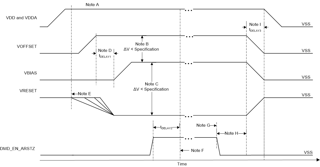
- During power-down, VDD and VDDA must be supplied until after VBIAS, VRESET, and VOFFSET are discharged to within the specified limit of ground. See Table 9-2.
- During power-down, it is a strict requirement that the voltage difference between VBIAS and VOFFSET must be within the specified limit shown in Section 6.4.
- During power-down, there is no requirement for the relative timing of VRESET with respect to VBIAS.
- Power supply slew rates during power-down are flexible, provided that the transient voltage levels follow the requirements specified in Section 6.1, in Section 6.4, and in Figure 9-1.
- During power-down, LVCMOS input pins must be less than specified in Section 6.4.

A. See Section 5 for the Pin Functions Table.
B. To prevent excess current, the
supply voltage difference |VOFFSET – VBIAS| must be less
than the specified limit in Section 6.4.
C. To prevent excess current, the
supply difference |VBIAS – VRESET| must be less than the
specified limit in Section 6.4.
D. VBIAS should power
up after VOFFSET has powered up, per
the
Delay1 specification in Table 9-2.
E. DLP controller software
initiates the global VBIAS command.
F. After the DMD micromirror park
sequence is complete, the DLP controller software initiates a hardware
power-down that activates DMD_EN_ARSTZ and disables VBIAS,
VRESET,
and VOFFSET.
G. Under power-loss conditions
where emergency DMD micromirror park procedures are being enacted by the DLP
controller hardware DMD_EN_ARSTZ will go low.
H. VDD must remain high
until after VOFFSET, VBIAS, VRESET go low, per
Delay2 specification in Table 9-2.
I. To prevent excess current, the
supply voltage delta |VDDA – VDD| must be less than
specified limit in Section 6.4.
Figure 9-1 DMD Power
Supply RequirementsTable 9-2 DMD Power-Supply Requirements
| PARAMETER | DESCRIPTION | MIN | NOM | MAX | UNIT |
|---|---|---|---|---|---|
| Delay1(1) | Delay from VOFFSET settled at recommended operating voltage to VBIAS and VRESET power up | 1 | 2 | ms | |
| Delay2(1) | Delay VDD must be held high from VOFFSET, VBIAS and VRESET powering down. | 50 | us |
(1) See Figure 9-1.