SLVSH22 May 2024 DRV8000-Q1
ADVANCE INFORMATION
- 1
- 1 Features
- 2 Applications
- 3 Description
- 4 Device Comparison
- 5 Pin Configuration and Functions
- 6 Specifications
-
7 Detailed Description
- 7.1 Overview
- 7.2 Functional Block Diagram
- 7.3 External Components
- 7.4
Feature Description
- 7.4.1 Heater MOSFET Driver
- 7.4.2 High-side Drivers
- 7.4.3 Electro-chromic Glass Driver
- 7.4.4 Half-bridge Drivers
- 7.4.5
Gate Drivers
- 7.4.5.1 Input PWM Modes
- 7.4.5.2
Smart Gate Driver - Functional Block
Diagram
- 7.4.5.2.1 Smart Gate Driver
- 7.4.5.2.2 Functional Block Diagram
- 7.4.5.2.3 Slew Rate Control (IDRIVE)
- 7.4.5.2.4 Gate Driver State Machine (TDRIVE)
- 7.4.5.2.5 Propagation Delay Reduction (PDR)
- 7.4.5.2.6 PDR Pre-Charge/Pre-Discharge Control Loop Operation Details
- 7.4.5.2.7 PDR Post-Charge/Post-Discharge Control Loop Operation Details
- 7.4.5.2.8 Detecting Drive and Freewheel MOSFET
- 7.4.5.2.9 Automatic Duty Cycle Compensation (DCC)
- 7.4.5.2.10 Closed Loop Slew Time Control (STC)
- 7.4.5.3 Tripler (Double-Stage) Charge Pump
- 7.4.5.4 Wide Common Mode Differential Current Shunt Amplifier
- 7.4.5.5 Gate Driver Protection Circuits
- 7.4.6 Sense Output (IPROPI)
- 7.4.7
Protection Circuits
- 7.4.7.1 Fault Reset (CLR_FLT)
- 7.4.7.2 DVDD Logic Supply Power on Reset (DVDD_POR)
- 7.4.7.3 PVDD Supply Undervoltage Monitor (PVDD_UV)
- 7.4.7.4 PVDD Supply Overvoltage Monitor (PVDD_OV)
- 7.4.7.5 VCP Charge Pump Undervoltage Lockout (VCP_UV)
- 7.4.7.6 Thermal Clusters
- 7.4.7.7 Watchdog Timer
- 7.4.7.8 Fault Detection and Response Summary Table
- 7.5 Programming
- 8 DRV8000-Q1 Register Map
- 9 DRV8000-Q1_STATUS Registers
- 10DRV8000-Q1_CNFG Registers
- 11DRV8000-Q1_CTRL Registers
- 12Application and Implementation
- 13Device and Documentation Support
- 14Revision History
- 15Mechanical, Packaging, and Orderable Information
7.4.5.2.5 Propagation Delay Reduction (PDR)
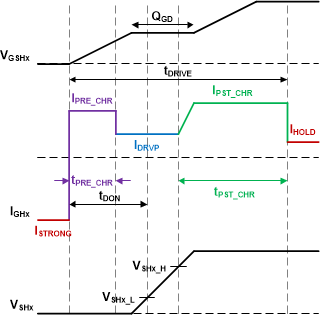
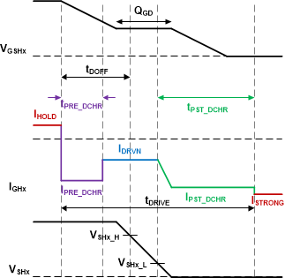
Propagation delay reduction (PDR) control has two primary functions, a pre-charge propagation delay reduction function and a post-charge acceleration function. The PDR control function is only available in the Section 7.4.4.1 PWM mode.
The propagation delay reduction (PDR) primary goal is to reduce the turn on and turn off delay of the external MOSFET by using dynamic pre-charge and pre-discharge currents before the MOSFET QGD miller region. This can enable the driver to achieve higher and lower duty cycle resolution while still meeting difficult EMI requirements.
The post-charge acceleration function allows for the MOSFET to more quickly reach its low resistive or off state to minimize power losses by increasing the post-charge and post-discharge gate current after the MOSFET QGD miller region.
An example of the MOSFET pre-charge and post-charge current profiles are shown in . The same control loop is repeated for the MOSFET pre-discharge and post-discharge as shown in PDR Charge Profile and PDR Discharge Profile. Several examples of the full control loop in different PWM and motor cases are shown in HS Drive PWM Turn On/Off Example and LS Drive PWM Turn On/Off Example.
 Figure 7-26 PDR Charge Profile
 Figure 7-27 PDR Discharge
Profile