JAJSLP6F June 2012 – April 2021 DRV8837 , DRV8838
PRODUCTION DATA
- 1 特長
- 2 アプリケーション
- 3 概要
- 4 Revision History
- 5 Pin Configuration and Functions
- 6 Specifications
- 7 Detailed Description
- 8 Power Supply Recommendations
- 9 Layout
- 10Device and Documentation Support
パッケージ・オプション
メカニカル・データ(パッケージ|ピン)
- DSG|8
サーマルパッド・メカニカル・データ
- DSG|8
発注情報
6.6 Timing Requirements
TA = 25°C, VM = 5 V, VCC = 3 V, RL = 20 Ω
| NO. | MIN | MAX | UNIT | |||
|---|---|---|---|---|---|---|
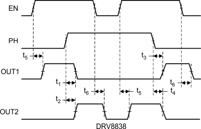
| 1 | t1 | Delay time, PHASE high to OUT1 low | See #SLVSBA45687. | 160 | ns | |
| 2 | t2 | Delay time, PHASE high to OUT2 high | 200 | ns | ||
| 3 | t3 | Delay time, PHASE low to OUT1 high | 200 | ns | ||
| 4 | t4 | Delay time, PHASE low to OUT2 low | 160 | ns | ||
| 5 | t5 | Delay time, ENBL high to OUTx high | 200 | ns | ||
| 6 | t6 | Delay time, ENBL low to OUTx low | 160 | ns | ||
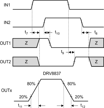
| 7 | t7 | Output enable time | See #SLVSBA4401. | 300 | ns | |
| 8 | t8 | Output disable time | 300 | ns | ||
| 9 | t9 | Delay time, INx high to OUTx high | 160 | ns | ||
| 10 | t10 | Delay time, INx low to OUTx low | 160 | ns | ||
| 11 | t11 | Output rise time | 30 | 188 | ns | |
| 12 | t12 | Output fall time | 30 | 188 | ns | |
| twake | Wake time, nSLEEP rising edge to part active | 30 | μs | |||
 Figure 6-1 Input and Output Timing for DRV8838
 Figure 6-2 Input and Output Timing for DRV8837