JAJS518G May 2004 – January 2015 INA193 , INA194 , INA195 , INA196 , INA197 , INA198
PRODUCTION DATA.
- 1 特長
- 2 アプリケーション
- 3 概要
- 4 改訂履歴
- 5 Device Comparison Table
- 6 Pin Configuration and Functions
- 7 Specifications
- 8 Detailed Description
- 9 Application and Implementation
- 10Power Supply Recommendations
- 11Layout
- 12デバイスおよびドキュメントのサポート
- 13メカニカル、パッケージ、および注文情報
8 Detailed Description
8.1 Overview
The INA193−INA198 family of current shunt monitors with voltage output can sense drops across shunts at common-mode voltages from −16 V to +80 V, independent of the INA19x supply voltage. They are available with three output voltage scales: 20 V/V, 50 V/V, and 100 V/V. The 500-kHz bandwidth simplifies use in current control loops. The INA193−INA195 devices provide identical functions but alternative pin configurations to the INA196−INA198, respectively.
The INA193−INA198 devices operate from a single +2.7-V to +18-V supply, drawing a maximum of 900 μA of supply current. They are specified over the extended operating temperature range (−40°C to +125°C), and are offered in a space-saving SOT-23 package.
8.2 Functional Block Diagram

8.3 Feature Description
8.3.1 Basic Connection
Figure 20 shows the basic connection of the INA193-INA198. To minimize any resistance in series with the shunt resistance, connect the input pins, VIN+ and VIN−, as closely as possible to the shunt resistor.
Power-supply bypass capacitors are required for stability. Applications with noisy or high impedance power supplies may require additional decoupling capacitors to reject power-supply noise. Connect bypass capacitors close to the device pins.
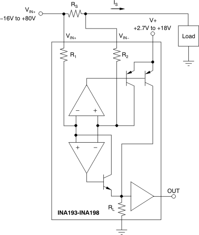 Figure 20. INA193-INA198 Basic Connection
8.3.2 Selecting RS
The value chosen for the shunt resistor, RS, depends on the application and is a compromise between small-signal accuracy and maximum permissible voltage loss in the measurement line. High values of RS provide better accuracy at lower currents by minimizing the effects of offset, while low values of RS minimize voltage loss in the supply line. For most applications, best performance is attained with an RS value that provides a full-scale shunt voltage range of 50 mV to 100 mV. Maximum input voltage for accurate measurements is 500 mV.
8.3.3 Inside the INA193-INA198
The INA193-INA198 devices use a new, unique internal circuit topology that provides common-mode range extending from −16 to 80 V while operating from a single power supply. The common-mode rejection in a classic instrumentation amplifier approach is limited by the requirement for accurate resistor matching. By converting the induced input voltage to a current, the INA193-INA198 devices provide common-mode rejection that is no longer a function of closely matched resistor values, providing the enhanced performance necessary for such a wide common-mode range. A simplified diagram (shown in Figure 21) shows the basic circuit function. When the common-mode voltage is positive, amplifier A2 is active.
The differential input voltage, (VIN+) − (VIN−) applied across RS, is converted to a current through a resistor. This current is converted back to a voltage through RL, and then amplified by the output buffer amplifier. When the common-mode voltage is negative, amplifier A1 is active. The differential input voltage, (VIN+) − (VIN−) applied across RS, is converted to a current through a resistor. This current is sourced from a precision current mirror whose output is directed into RL converting the signal back into a voltage and amplified by the output buffer amplifier. Patent-pending circuit architecture ensures smooth device operation, even during the transition period where both amplifiers A1 and A2 are active.
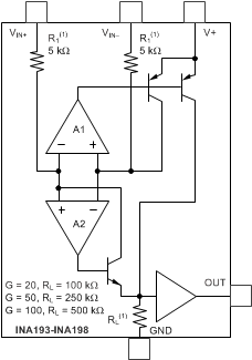
NOINDENT:
Nominal resistor values are shown. ±15% variation is possible. Resistor ratios are matched to ±1%.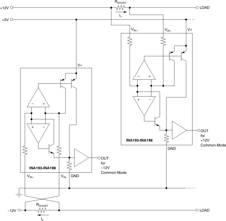 Figure 22. Monitor Bipolar Output Power-Supply Current
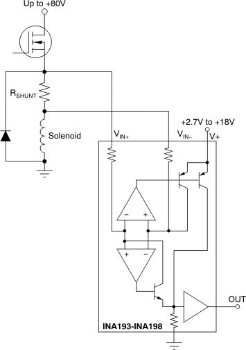 Figure 23. Inductive Current Monitor Including Flyback
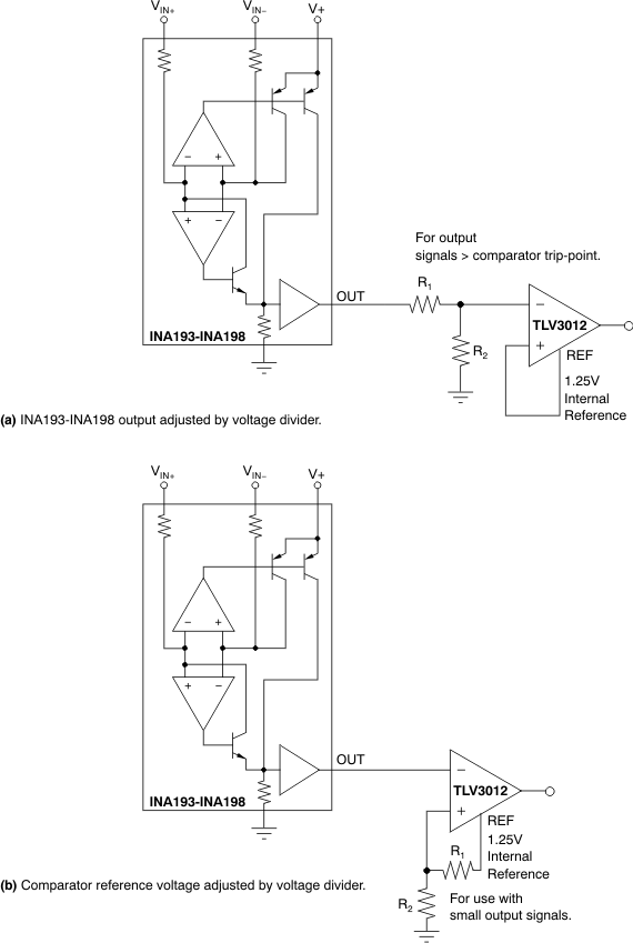 Figure 24. INA193-INA198 with Comparator
8.4 Device Functional Modes
8.4.1 Input Filtering
An obvious and straightforward location for filtering is at the output of the INA193-INA198 devices; however, this location negates the advantage of the low output impedance of the internal buffer. The only other option for filtering is at the input pins of the INA193-INA198 devices, which is complicated by the internal 5-kΩ + 30% input impedance; this is illustrated in Figure 25. Using the lowest possible resistor values minimizes both the initial shift in gain and effects of tolerance. The effect on initial gain is given by Equation 1:

Total effect on gain error can be calculated by replacing the 5-kΩ term with 5 kΩ − 30%, (or 3.5 kΩ) or 5 kΩ + 30% (or 6.5 kΩ). The tolerance extremes of RFILT can also be inserted into the equation. If a pair of 100-Ω 1% resistors are used on the inputs, the initial gain error will be approximately 2%. Worst-case tolerance conditions will always occur at the lower excursion of the internal 5-kΩ resistor (3.5 kΩ), and the higher excursion of RFILT − 3% in this case.
Note that the specified accuracy of the INA193-INA198 devices must then be combined in addition to these tolerances. While this discussion treated accuracy worst-case conditions by combining the extremes of the resistor values, it is appropriate to use geometric mean or root sum square calculations to total the effects of accuracy variations.
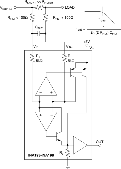 Figure 25. Input Filter (Gain Error − 1.5% To −2.2%)
8.4.2 Accuracy Variations as a Result of VSENSE and Common-Mode Voltage
The accuracy of the INA193−INA198 current shunt monitors is a function of two main variables: VSENSE (VIN+ − VIN−) and common-mode voltage, VCM, relative to the supply voltage, VS. VCM is expressed as (VIN+ + VIN−)/2; however, in practice, VCM is seen as the voltage at VIN+ because the voltage drop across VSENSE is usually small.
This section addresses the accuracy of these specific operating regions:
Normal Case 1: VSENSE ≥ 20mV, VCM ≥ VS
Normal Case 2: VSENSE ≥ 20mV, VCM < VS
Low VSENSE Case 1: VSENSE < 20mV, −16V ≤ VCM < 0
Low VSENSE Case 2: VSENSE < 20mV, 0V ≤ VCM ≤ VS
Low VSENSE Case 3: VSENSE < 20mV, VS < VCM ≤ 80V
8.4.2.1 Normal Case 1: VSENSE ≥ 20mv, VCM ≥ VS
This region of operation provides the highest accuracy. Here, the input offset voltage is characterized and measured using a two-step method. First, the gain is determined by Equation 2.

where
Then the offset voltage is measured at VSENSE = 100mV and referred to the input (RTI) of the current shunt monitor, as shown in Equation 3.

In the Typical Characteristics, the Output Error vs Common-Mode Voltage curve (Figure 6) shows the highest accuracy for this region of operation. In this plot, VS = 12 V; for VCM ≥ 12 V, the output error is at its minimum. This case is also used to create the VSENSE ≥ 20-mV output specifications in the Electrical Characteristics table.
8.4.2.2 Normal Case 2: VSENSE ≥ 20mv, VCM < VS
This region of operation has slightly less accuracy than Normal Case 1 as a result of the common-mode operating area in which the part functions, as seen in the Output Error vs Common-Mode Voltage curve (Figure 6). As noted, for this graph VS = 12 V; for VCM < 12 V, the Output Error increases as VCM becomes less than 12 V, with a typical maximum error of 0.005% at the most negative VCM = −16V.
8.4.2.3 Low VSENSE Case 1: VSENSE < 20mV, −16v ≤ VCM < 0; and Low VSENSE Case 3: VSENSE < 20mV, VS < VCM ≤ 80V
Although the INA193−INA198 family of devices are not designed for accurate operation in either of these regions, some applications are exposed to these conditions; for example, when monitoring power supplies that are switched on and off while VS is still applied to the INA193−INA198 devices. It is important to know what the behavior of the devices will be in these regions.
As VSENSE approaches 0 mV, in these VCM regions, the device output accuracy degrades. A larger-than-normal offset can appear at the current shunt monitor output with a typical maximum value of VOUT = 300 mV for VSENSE = 0 mV. As VSENSE approaches 20 mV, VOUT returns to the expected output value with accuracy as specified in the Electrical Characteristics. Figure 26 illustrates this effect using the INA195 and INA198 devices (Gain = 100).
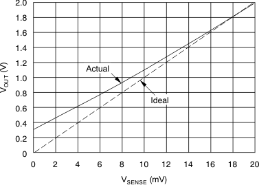 Figure 26. Example for Low VSENSE Cases 1 and 3 (INA195, INA198: Gain = 100)
8.4.2.4 Low VSENSE Case 2: VSENSE < 20 mV, 0 V ≤ VCM ≤ VS
This region of operation is the least accurate for the INA193−INA198 family of devices. To achieve the wide input common-mode voltage range, these devices use two op amp front ends in parallel. One op amp front end operates in the positive input common-mode voltage range, and the other in the negative input region. For this case, neither of these two internal amplifiers dominates and overall loop gain is very low. Within this region, VOUT approaches voltages close to linear operation levels for Normal Case 2. This deviation from linear operation becomes greatest the closer VSENSE approaches 0 V. Within this region, as VSENSE approaches 20 mV, device operation is closer to that described by Normal Case 2. Figure 27 illustrates this behavior for the INA195 device. The VOUT maximum peak for this case is tested by maintaining a constant VS, setting VSENSE = 0 mV and sweeping VCM from 0 V to VS. The exact VCM at which VOUT peaks during this test varies from part to part, but the VOUT maximum peak is tested to be less than the specified VOUT Tested Limit.
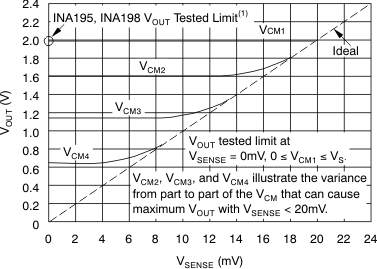
NOINDENT:
INA193, INA196 VOUT Tested Limit = 0.4V. INA194, INA197 VOUT Tested Limit = 1V.8.4.3 Shutdown
Because the INA193-INA198 devices consume a quiescent current less than 1 mA, they can be powered by either the output of logic gates or by transistor switches to supply power. Use a totem-pole output buffer or gate that can provide sufficient drive along with 0.1-μF bypass capacitor, preferably ceramic with good high-frequency characteristics. This gate should have a supply voltage of 3 V or greater because the INA193-INA198 devices require a minimum supply greater than 2.7 V. In addition to eliminating quiescent current, this gate also turns off the 10-μA bias current present at each of the inputs. An example shutdown circuit is shown in Figure 28.
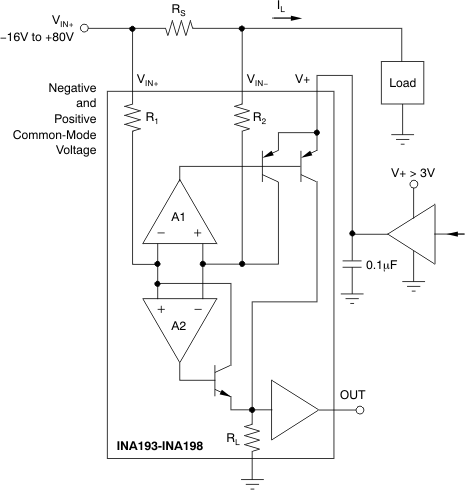 Figure 28. INA193-INA198 Example Shutdown Circuit
8.4.4 Transient Protection
The −16-V to +80-V common-mode range of the INA193-INA198 devices is ideal for withstanding automotive fault conditions ranging from 12-V battery reversal up to 80-V transients, since no additional protective components are needed up to those levels. In the event that the INA193-INA198 devices are exposed to transients on the inputs in excess of its ratings, then external transient absorption with semiconductor transient absorbers (zeners or Transzorbs) will be necessary. Use of MOVs or VDRs is not recommended except when they are used in addition to a semiconductor transient absorber. Select the transient absorber such that it will never allow the INA193-INA198 devices to be exposed to transients greater than +80 V (that is, allow for transient absorber tolerance, as well as additional voltage due to transient absorber dynamic impedance). Despite the use of internal zener-type ESD protection, the INA193-INA198 devices do not lend themselves to using external resistors in series with the inputs because the internal gain resistors can vary up to ±30%. (If gain accuracy is not important, then resistors can be added in series with the INA193-INA198 inputs with two equal resistors on each input.)
8.4.5 Output Voltage Range
The output of the INA193-INA198 devices are accurate within the output voltage swing range set by the power-supply pin, V+. This is best illustrated when using the INA195 or INA198 devices (which are both versions using a gain of 100), where a 100-mV full-scale input from the shunt resistor requires an output voltage swing of +10 V, and a power-supply voltage sufficient to achieve +10 V on the output.