JAJSCM0C April   2011  – April 2016 INA200-Q1 , INA201-Q1 , INA202-Q1

PRODUCTION DATA.  

  1. 特長
  2. アプリケーション
  3. 概要
  4. 改訂履歴
  5. Device Comparison Table
  6. Pin Configuration and Functions
  7. Specifications
    1. 7.1 Absolute Maximum Ratings
    2. 7.2 ESD Ratings
    3. 7.3 Recommended Operating Conditions
    4. 7.4 Thermal Information
    5. 7.5 Electrical Characteristics: Current-Shunt Monitor
    6. 7.6 Electrical Characteristics: Comparator
    7. 7.7 Electrical Characteristics: General
    8. 7.8 Typical Characteristics
  8. Parameter Measurement Information
    1. 8.1 Hysteresis
  9. Detailed Description
    1. 9.1 Overview
    2. 9.2 Functional Block Diagram
    3. 9.3 Feature Description
      1. 9.3.1 Comparator
      2. 9.3.2 Output Voltage Range
    4. 9.4 Device Functional Modes
  10. 10Application Information
    1. 10.1 Application Information
      1. 10.1.1 Basic Connections
      2. 10.1.2 Selecting RS
      3. 10.1.3 Input Filtering
      4. 10.1.4 Accuracy Variations as a Result of VSENSE and Common-Mode Voltage
        1. 10.1.4.1 Normal Case 1: VSENSE ≥ 20 mV, VCM ≥ VS
        2. 10.1.4.2 Normal Case 2: VSENSE ≥ 20 mV, VCM < VS
        3. 10.1.4.3 Low VSENSE Case 1: VSENSE < 20 mV, -16 V ≤ VCM < 0 V; and Low VSENSE Case 3: VSENSE < 20 mV, VS < VCM ≤ 80 V
        4. 10.1.4.4 Low VSENSE Case 2: VSENSE < 20 mV, 0 V ≤ VCM ≤ VS
      5. 10.1.5 Transient Protection
    2. 10.2 Typical Applications
      1. 10.2.1 Low-Side Switch Overcurrent Shutdown
        1. 10.2.1.1 Design Requirements
        2. 10.2.1.2 Detailed Design Procedure
        3. 10.2.1.3 Application Curves
      2. 10.2.2 High-Side Switch Overcurrent Shutdown
      3. 10.2.3 Bidirectional Overcurrent Comparator
  11. 11Power Supply Recommendations
  12. 12Layout
    1. 12.1 Layout Guidelines
    2. 12.2 Layout Example
  13. 13デバイスおよびドキュメントのサポート
    1. 13.1 関連リンク
    2. 13.2 コミュニティ・リソース
    3. 13.3 商標
    4. 13.4 静電気放電に関する注意事項
    5. 13.5 Glossary
  14. 14メカニカル、パッケージ、および注文情報

パッケージ・オプション

メカニカル・データ(パッケージ|ピン)
サーマルパッド・メカニカル・データ
発注情報

Layout

Layout Guidelines

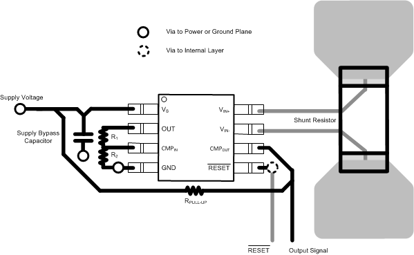
  • Connect the input pins to the sensing resistor using a Kelvin or four-wire connection. This connection technique makes sure that only the current-sensing resistor impedance is detected between the input pins. Poor routing of the current-sensing resistor commonly results in additional resistance present between the input pins. Given the very low ohmic value of the current resistor, any additional high-current carrying impedance can cause significant measurement errors.
  • Place the power-supply bypass capacitor as close as possible to the supply and ground pins. The recommended value of this bypass capacitor is 0.1 μF. Add additional decoupling capacitance to compensate for noisy or high-impedance power supplies.

Layout Example

INA200-Q1 INA201-Q1 INA202-Q1 pcblayout.gif Figure 35. INA20x-Q1 Layout Example