JAJSOS4K December 2008 – June 2022 LM25088 , LM25088-Q1
PRODUCTION DATA
- 1 特長
- 2 アプリケーション
- 3 概要
- 4 Revision History
- 5 Pin Configuration and Functions
- 6 Specifications
-
7 Detailed Description
- 7.1 Overview
- 7.2 Functional Block Diagram
- 7.3
Feature Description
- 7.3.1 High Voltage Low-Dropout Regulator
- 7.3.2 Line Undervoltage Detector
- 7.3.3 Oscillator and Sync Capability
- 7.3.4 Error Amplifier and PWM Comparator
- 7.3.5 Ramp Generator
- 7.3.6 Dropout Voltage Reduction
- 7.3.7 Frequency Dithering (LM25088-1 Only)
- 7.3.8 Cycle-by-Cycle Current Limit
- 7.3.9 Overload Protection Timer (LM25088-2 Only)
- 7.3.10 Soft Start
- 7.3.11 HG Output
- 7.3.12 Thermal Protection
- 7.4 Device Functional Modes
-
8 Application and Implementation
- 8.1 Application Information
- 8.2
Typical Application
- 8.2.1 Design Requirements
- 8.2.2
Detailed Design Procedure
- 8.2.2.1 Timing Resistor
- 8.2.2.2 Output Inductor
- 8.2.2.3 Current Sense Resistor
- 8.2.2.4 Ramp Capacitor
- 8.2.2.5 Output Capacitors
- 8.2.2.6 Input Capacitors
- 8.2.2.7 VCC Capacitor
- 8.2.2.8 Bootstrap Capacitor
- 8.2.2.9 Soft-Start Capacitor
- 8.2.2.10 Output Voltage Divider
- 8.2.2.11 UVLO Divider
- 8.2.2.12 Restart Capacitor (LM5008-2 Only)
- 8.2.2.13 MOSFET Selection
- 8.2.2.14 Diode Selection
- 8.2.2.15 Snubber Components Selection
- 8.2.2.16 Error Amplifier Compensation
- 8.2.3 Application Curves
- 9 Power Supply Recommendations
- 10Layout
- 11Device and Documentation Support
- 12Mechanical, Packaging, and Orderable Information
パッケージ・オプション
メカニカル・データ(パッケージ|ピン)
- PWP|16
サーマルパッド・メカニカル・データ
- PWP|16
発注情報
8.2.2.16 Error Amplifier Compensation
RCOMP, CCOMP, and CHF configure the error amplifier gain characteristics to accomplish a stable voltage loop gain. One advantage of current mode control is the ability to close the loop with only two feedback components, RCOMP and CCOMP. The voltage loop gain is the product of the modulator gain and the error amplifier gain. For this example, the modulator can be treated as an ideal voltage-to-current (transconductance) converter. The DC modulator gain of the LM25088 can be modeled as:
The dominant low frequency pole of the modulator is determined by the load resistance (RLOAD) and the output capacitance (COUT). The corner frequency of this pole is:
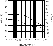
For the 5-V design example, the modulator gain versus frequency characteristic was measured as shown in Figure 8-4.
 Figure 8-4 Modular Gain Phase
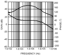
Components RCOMP and CCOMP configure the error amplifier as a type II compensation configuration. The DC gain of the amplifier is 80 dB, which has a pole at low frequency and a zero at fZero = 1 / (2π × RCOMP × CCOMP). The error amplifier zero is set such that it cancels the modulator pole, leaving a single pole response at the crossover frequency of the voltage loop. A single pole response at the crossover frequency yields a very stable loop with 90° of phase margin. For the design example, a target loop bandwidth (crossover frequency) of 15 kHz was selected. The compensation network zero (fZero) must be at least an order of magnitude lower than the target crossover frequency. This restriction constrains the product of RCOMP and CCOMP for a desired compensation network zero 1/ (2π × RCOMP × CCOMP) to be less than 1.5 kHz. Increasing RCOMP, while proportionally decreasing CCOMP, decreases the error amp gain. For the design example, CCOMP was selected to be 0.015 µF and RCOMP was selected to be 18 kΩ. These values configure the compensation network zero at 0.6 kHz. The error amp gain at frequencies greater than fZero is RCOMP / RFB2, which is approximately 3.56 (11 dB).
 Figure 8-5 Error Amplifier Gain and Phase
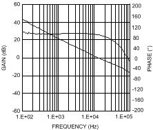
The overall voltage loop gain can be predicted as the sum (in dB) of the modulator gain and the error amp gain. If a network analyzer is available, the modulator gain can be measured and the error amplifier gain can be configured for the desired loop transfer function. If a network analyzer is not available, the error amplifier compensation components can be designed with the suggested guidelines. Step load transient tests can be performed to verify performance. The step load goal is minimum overshoot with a damped response. CHF can be added to the compensation network to decrease noise susceptibility of the error amplifier. The value of CHF must be sufficiently small since the addition of this capacitor adds a pole in the error amplifier transfer function. A good approximation of the location of the pole added by CHF is fP2 = fZero × CCOMP / CHF. Using CHF is recommended to minimize coupling of any switching noise into the modulator. The value of CHF was selected as 100 pF for this design example.
 Figure 8-6 Overall Loop Gain and Phase