JAJSOS4K December 2008 – June 2022 LM25088 , LM25088-Q1
PRODUCTION DATA
- 1 特長
- 2 アプリケーション
- 3 概要
- 4 Revision History
- 5 Pin Configuration and Functions
- 6 Specifications
-
7 Detailed Description
- 7.1 Overview
- 7.2 Functional Block Diagram
- 7.3
Feature Description
- 7.3.1 High Voltage Low-Dropout Regulator
- 7.3.2 Line Undervoltage Detector
- 7.3.3 Oscillator and Sync Capability
- 7.3.4 Error Amplifier and PWM Comparator
- 7.3.5 Ramp Generator
- 7.3.6 Dropout Voltage Reduction
- 7.3.7 Frequency Dithering (LM25088-1 Only)
- 7.3.8 Cycle-by-Cycle Current Limit
- 7.3.9 Overload Protection Timer (LM25088-2 Only)
- 7.3.10 Soft Start
- 7.3.11 HG Output
- 7.3.12 Thermal Protection
- 7.4 Device Functional Modes
-
8 Application and Implementation
- 8.1 Application Information
- 8.2
Typical Application
- 8.2.1 Design Requirements
- 8.2.2
Detailed Design Procedure
- 8.2.2.1 Timing Resistor
- 8.2.2.2 Output Inductor
- 8.2.2.3 Current Sense Resistor
- 8.2.2.4 Ramp Capacitor
- 8.2.2.5 Output Capacitors
- 8.2.2.6 Input Capacitors
- 8.2.2.7 VCC Capacitor
- 8.2.2.8 Bootstrap Capacitor
- 8.2.2.9 Soft-Start Capacitor
- 8.2.2.10 Output Voltage Divider
- 8.2.2.11 UVLO Divider
- 8.2.2.12 Restart Capacitor (LM5008-2 Only)
- 8.2.2.13 MOSFET Selection
- 8.2.2.14 Diode Selection
- 8.2.2.15 Snubber Components Selection
- 8.2.2.16 Error Amplifier Compensation
- 8.2.3 Application Curves
- 9 Power Supply Recommendations
- 10Layout
- 11Device and Documentation Support
- 12Mechanical, Packaging, and Orderable Information
パッケージ・オプション
メカニカル・データ(パッケージ|ピン)
- PWP|16
サーマルパッド・メカニカル・データ
- PWP|16
発注情報
9.1 Thermal Considerations
In a buck converter, most of the losses can be attributed to MOSFET conduction and switching loss, re-circulating diode conduction loss, inductor DCR loss, and LM25088 VIN and VCC loss. The other dissipative components in a buck converter produce losses but these other losses collectively account for about 2% of the total loss. Formulas to calculate all the major losses are described in their respective sections of this data sheet. The easiest method to determine the power dissipated within the LM25088 is to measure the total conversion losses (PIN – POUT), then subtract the power losses in the Schottky diode, MOSFET, output inductor, and snubber resistor. When operating at 7 A of output current and at 36 V, the power dissipation of the LM25088 is approximately 550 mW. The junction-to-ambient thermal resistance of the LM25088 mounted in the evaluation board is approximately 40°C with no airflow. At 25°C ambient temperature and no airflow, the predicted junction temperature is 25 + 40 × 0.55 = 47°C. The LM25088 has an exposed thermal pad to aid in power dissipation. Adding several vias under the device greatly reduces the controller junction temperature. The junction to ambient thermal resistance varies with application. The most significant variables are the area of copper in the PC board; the number of vias under the IC exposed pad and the amount of forced air cooling. The integrity of solder connection from the IC exposed pad to the PC board is critical. Excessive voids greatly diminish the thermal dissipation capacity.
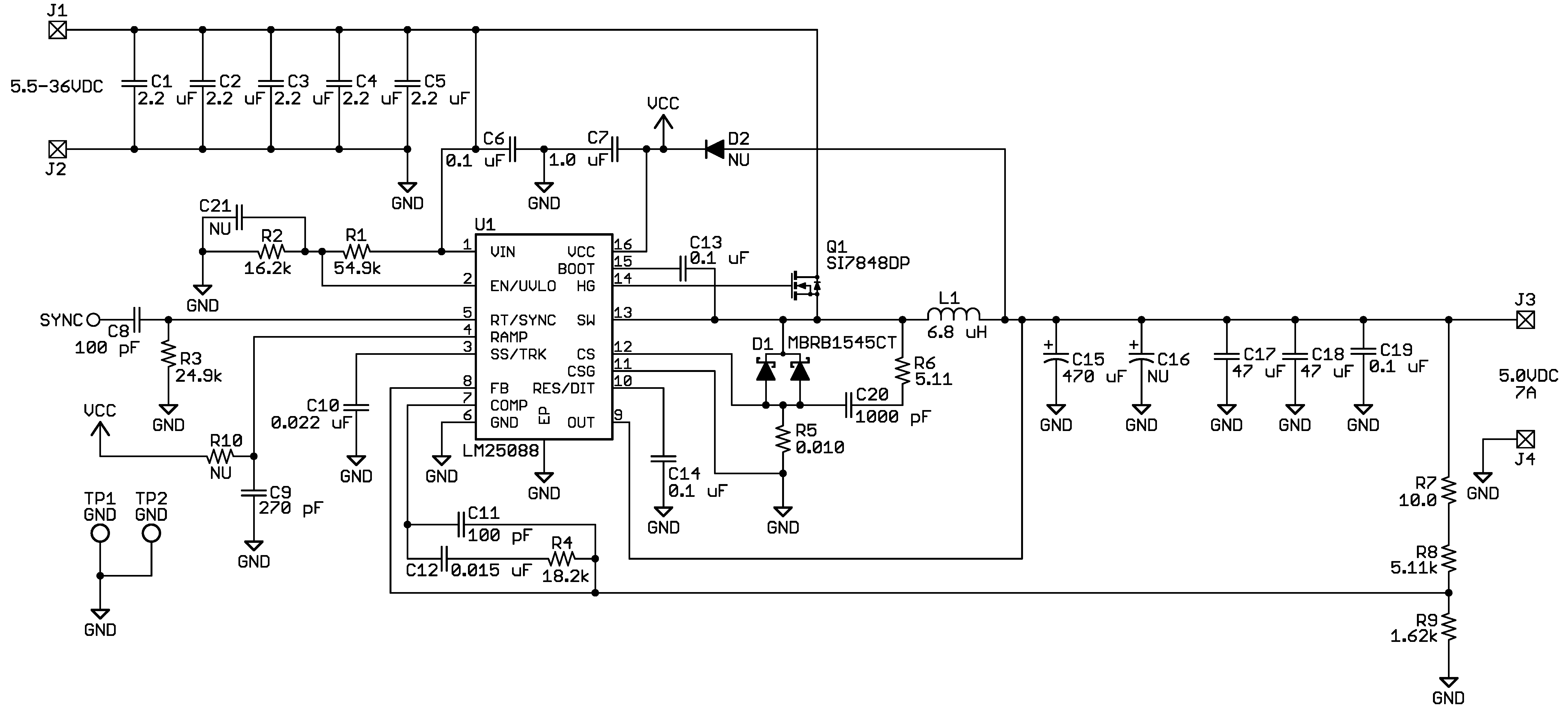
 Figure 9-1 LM25088-1 Application
Schematic
 Figure 9-2 LM25088-2 Application
Schematic