JAJSAY1E March 2008 – October 2017 LM2854
PRODUCTION DATA.
- 1 特長
- 2 アプリケーション
- 3 概要
- 4 改訂履歴
- 5 Pin Configuration and Functions
- 6 Specifications
- 7 Detailed Description
-
8 Application and Implementation
- 8.1 Application Information
- 8.2
Typical Application
- 8.2.1 Design Requirements
- 8.2.2
Detailed Design Procedure
- 8.2.2.1 Input Filter Capacitor
- 8.2.2.2 AVIN Filtering Components
- 8.2.2.3 Soft-Start Capacitor
- 8.2.2.4 Tracking - Equal Soft-Start Time
- 8.2.2.5 Tracking - Equal Slew Rates
- 8.2.2.6 Enable and UVLO
- 8.2.2.7 Output Voltage Setting
- 8.2.2.8 Compensation Component Selection
- 8.2.2.9 Filter Inductor and Output Capacitor Selection
- 8.2.3 Application Curves
- 8.2.4 System Examples
- 9 Power Supply Recommendations
- 10Layout
- 11デバイスおよびドキュメントのサポート
- 12メカニカル、パッケージ、および注文情報
パッケージ・オプション
メカニカル・データ(パッケージ|ピン)
- PWP|16
サーマルパッド・メカニカル・データ
- PWP|16
発注情報
8.2.2.8 Compensation Component Selection
The power stage transfer function of a voltage mode buck converter has a complex double pole related to the LC output filter and a left half plane zero due to the output capacitor ESR, denoted RESR. The locations of these singularities are given respectively in Equation 12.

where
- CO is the output capacitance value appropriately derated for applied voltage and operating temperature
- RL is the effective load resistance
- RDCR is the series damping resistance associated with the inductor and power switches
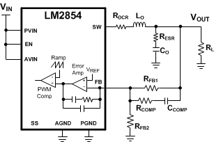
 Figure 21. LM2854 Compensation Scheme
The conventional compensation strategy employed with voltage mode control is to use two compensator zeros to offset the LC double pole, one compensator pole located to cancel the output capacitor ESR zero and one compensator pole located between one third and one half switching frequency for high frequency noise attenuation.
The LM2854 internal compensation components are designed to locate a pole at the origin and a pole at high frequency as mentioned above. Furthermore, a zero is located at 8.8 kHz or 17.6 kHz for the 500 kHz or 1 MHz options, respectively, to approximately cancel the likely location of one LC filter pole.
The three external compensation components, RFB1, RCOMP and CCOMP, are selected to position a zero at or below the LC pole location and a pole to cancel the ESR zero. The voltage loop crossover frequency, floop, is usually selected between one tenth to one fifth of the switching frequency, as shown in Equation 13.
A simple solution for the required external compensation capacitor, CCOMP, with type III voltage mode control can be expressed as in Equation 14.

where the constant α is nominally 0.038 or 0.075 for the 500 kHz or 1 MHz options, respectively. This assumes a compensator pole cancels the output capacitor ESR zero. Furthermore, since the modulator gain is proportional to VIN, the loop crossover frequency increases with VIN. Thus, it is recommended to design the loop at maximum expected VIN.
The upper feedback resistor, RFB1, is selected to provide adequate mid-band gain and to locate a zero at or below the LC pole frequency. The series resistor, RCOMP, is selected to locate a pole at the ESR zero frequency, as shown in Equation 15.

Note that the lower feedback resistor, RFB2, has no impact on the control loop from an AC standpoint since the FB pin is the input to an error amplifier and effectively at AC ground. Hence, the control loop can be designed irrespective of output voltage level. The only caveat here is the necessary derating of the output capacitance with applied voltage. Having chosen RFB1 as above, RFB2 is then selected for the desired output voltage.
Table 1 and Table 2 list inductor and ranges of capacitor values that work well with the LM2854, along with the associated compensation components to ensure stable operation. Values different than those listed may be used, but the compensation components may need to be recalculated to avoid degradation in phase margin. Note that the capacitance ranges specified refer to in-circuit values where the nominal capacitance value is adequately derated for applied voltage.