JAJSAH6H January   2006  – October 2017 LM3100

PRODUCTION DATA.  

  1. 特長
  2. アプリケーション
  3. 概要
    1.     Device Images
      1.      代表的なアプリケーション
  4. 改訂履歴
  5. Pin Configuration and Functions
    1.     Pin Functions
  6. Specifications
    1. 6.1 Absolute Maximum Ratings
    2. 6.2 ESD Ratings
    3. 6.3 Recommended Operating Conditions
    4. 6.4 Thermal Information
    5. 6.5 Electrical Characteristics
    6. 6.6 Typical Characteristics
  7. Detailed Description
    1. 7.1 Overview
    2. 7.2 Functional Block Diagram
    3. 7.3 Feature Description
      1. 7.3.1 Hysteretic Control Circuit Overview
    4. 7.4 Device Functional Modes
      1. 7.4.1 Start-up Regulator (VCC)
      2. 7.4.2 Regulation Comparator
      3. 7.4.3 Over-Voltage Comparator
      4. 7.4.4 ON-Time Timer, Shutdown
      5. 7.4.5 Current Limit
      6. 7.4.6 N-Channel Buck Switch and Driver
      7. 7.4.7 Soft-Start
      8. 7.4.8 Thermal Protection
  8. Applications and Implementation
    1. 8.1 Applications Information
      1. 8.1.1 External Components
        1. 8.1.1.1 RFB1 and RFB2
        2. 8.1.1.2 RON
        3. 8.1.1.3 L
        4. 8.1.1.4 CVCC
        5. 8.1.1.5 CO and CO3
        6. 8.1.1.6 CIN and CIN3
        7. 8.1.1.7 CBST
        8. 8.1.1.8 CSS
        9. 8.1.1.9 CFB
    2. 8.2 Typical Application
  9. Layout
    1. 9.1 Layout Guidelines
      1. 9.1.1 PC Board Layout
  10. 10デバイスおよびドキュメントのサポート
    1. 10.1 ドキュメントの更新通知を受け取る方法
    2. 10.2 コミュニティ・リソース
    3. 10.3 商標
    4. 10.4 静電気放電に関する注意事項
    5. 10.5 Glossary
  11. 11メカニカル、パッケージ、および注文情報

パッケージ・オプション

メカニカル・データ(パッケージ|ピン)
サーマルパッド・メカニカル・データ
発注情報

L

The main parameter affected by the inductor is the output current ripple amplitude (IOR). The maximum allowable (IOR) must be determined at both the minimum and maximum nominal load currents. At minimum load current, the lower peak must not reach 0 A. At maximum load current, the upper peak must not exceed the current limit threshold (1.9 A). The allowable ripple current is calculated from the following equations:

Equation 9. IOR(MAX1) = 2 x IO(min)

or

Equation 10. IOR(MAX2) = 2 x (1.9 A - IO(max))

The lesser of the two ripple amplitudes calculated above is then used in the following equation:

Equation 11. LM3100 20174713.gif

where VIN is the maximum input voltage and Fs is determined from Equation 1. This provides a value for L. The next larger standard value should be used. L should be rated for the IPK current level shown in Figure 20.
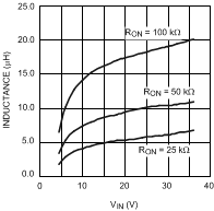
LM3100 20174736.gifFigure 22. Inductor Selector for VOUT = 3.3 V
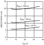
LM3100 20174737.gifFigure 23. Inductor Selector for VOUT = 0.8 V