JAJSB23D September 2010 – October 2016 LM3492 , LM3492-Q1
PRODUCTION DATA.
- 1 特長
- 2 アプリケーション
- 3 概要
- 4 改訂履歴
- 5 概要(続き)
- 6 Pin Configuration and Functions
- 7 Specifications
-
8 Detailed Description
- 8.1 Overview
- 8.2 Functional Block Diagram
- 8.3 Feature Description
- 8.4 Device Functional Modes
- 8.5 Programming
- 9 Application and Implementation
- 10Power Supply Recommendations
- 11Layout
- 12デバイスおよびドキュメントのサポート
- 13メカニカル、パッケージ、および注文情報
パッケージ・オプション
メカニカル・データ(パッケージ|ピン)
- PWP|20
サーマルパッド・メカニカル・データ
- PWP|20
発注情報
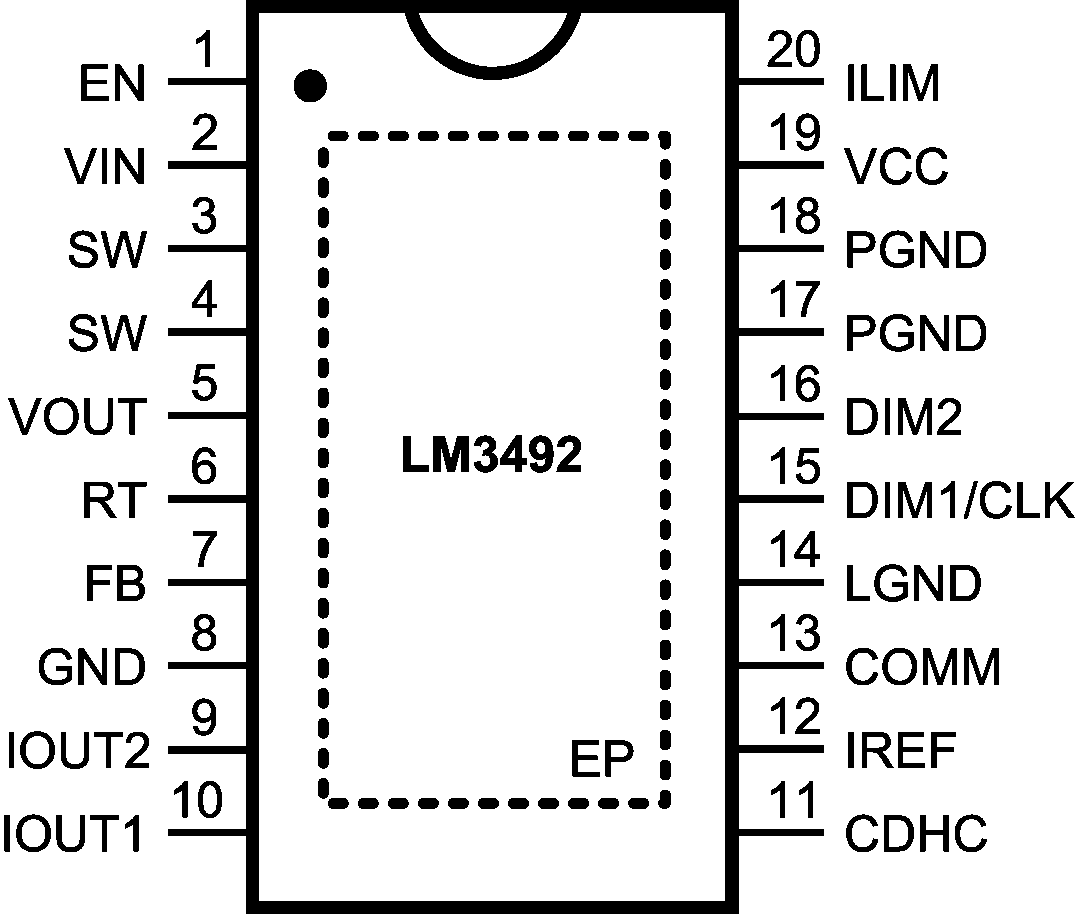
6 Pin Configuration and Functions
PWP PowerPAD™ Package
20-Pin HTSSOP
Top View

Pin Functions
| PIN | I/O | DESCRIPTION | APPLICATION INFORMATION | |
|---|---|---|---|---|
| NO. | NAME | |||
| 1 | EN | I | Enable | Internally pullup. Connect to a voltage higher than 1.63 V to provide precision enable for the device. |
| 2 | VIN | I | Input Supply Voltage | Supply pin to the device. Input range is 4.5 V to 65 V. |
| 3 | SW | I | Switch Node | Internally connected to the drain of the integrated MOSFET. |
| 4 | ||||
| 5 | VOUT | I | Output Voltage Sense | Sense the output voltage for nearly constant switching frequency control. |
| 6 | RT | I | Frequency Control | An external resistor from the VOUT pin to this pin sets the switching frequency. |
| 7 | FB | I | Output Voltage Feedback | The output voltage is connected to this pin through a feedback resistor divider for output voltage regulation. The voltage of this pin is from 1.05 V to 2.5 V. |
| 8 | GND | G | Analog Ground | Signal ground |
| 9 | IOUT2 | I | Current Regulator Input of Channel 2 | Input of the current regulator of channel 2. The regulated current is programmable (refer to the IREF pin). |
| 10 | IOUT1 | I | Current Regulator Input of Channel 1 | Input of the current regulator of channel 1. The regulated current is programmable (refer to the IREF pin). |
| 11 | CDHC | I | Dynamic Headroom Control |
An external capacitor connected to this pin sets the DHC sensitivity. At start-up, a 120-µA internal current source charges an external capacitor to provide a soft-start function. |
| 12 | IREF | I | Current Setting of the Current Regulator |
An external resistor connected from this pin to ground programs the regulated current of the current regulator of channels 1 and 2. |
| 13 | COMM | I/O | Bidirectional Logic Communication | This pin is open drain for various indications (power-good, overtemperature, IOUT overvoltage and undervoltage) and command sending (switching frequency tuning and channel 1 disabling). |
| 14 | LGND | G | Ground of the Current Regulator | Current regulator ground. Must be connected to the GND pin for normal operation. The LGND and GND pins are not internally connected. |
| 15 | DIM1/CLK | I/O | Dimming Control of Channel 1 |
Control the ON/OFF of the current regulator of channel 1. This pin is internally pulled low by a 5-µA current. This pin also serves as a clock signal for latching input/output data of the COMM pin. |
| 16 | DIM2 | I | Dimming Control of Channel 2 |
Control the ON/OFF of the current regulator of channel 2. This pin is internally pulled low by a 5-µA current. |
| 17 | PGND | G | Power Ground | Integrated MOSFET ground. Must be connected to the GND pin for normal operation. The PGND and GND pins are not internally connected. |
| 18 | ||||
| 19 | VCC | O | LDO Regulator Output | Nominally regulated to 5.5 V. Connect a capacitor of larger than 0.47 µF between the VCC and GND pins. |
| 20 | ILIM | I | Peak Current Limit Adjust | Connect an external resistor from the ILIM pin to the VCC pin reduces peak current limit. Connect the ILIM pin to the ground to obtain the maximum current limit. |
| DAP | DAP | — | Exposed Pad | Thermal connection pad. Connect to a ground plane. |