JAJSB23D September 2010 – October 2016 LM3492 , LM3492-Q1
PRODUCTION DATA.
- 1 特長
- 2 アプリケーション
- 3 概要
- 4 改訂履歴
- 5 概要(続き)
- 6 Pin Configuration and Functions
- 7 Specifications
-
8 Detailed Description
- 8.1 Overview
- 8.2 Functional Block Diagram
- 8.3 Feature Description
- 8.4 Device Functional Modes
- 8.5 Programming
- 9 Application and Implementation
- 10Power Supply Recommendations
- 11Layout
- 12デバイスおよびドキュメントのサポート
- 13メカニカル、パッケージ、および注文情報
パッケージ・オプション
メカニカル・データ(パッケージ|ピン)
- PWP|20
サーマルパッド・メカニカル・データ
- PWP|20
発注情報
8 Detailed Description
8.1 Overview
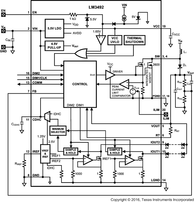
The LM3492/-Q1 integrates a boost converter and a two-channel current regulator to implement a high efficient and cost effective LED driver for driving two individually dimmable LED strings with a maximum power of 15 W and an output voltage of up to 65 V. The boost converter provides power for the LED strings, and the current regulator controls the dimming of the LED strings individually. The LM3492/-Q1 integrates an N-channel MOSFET switch and a two-channel current regulator to minimize the component count and solution size.
The boost converter of the LM3492/-Q1 employs a Projected On-Time (POT) control method to determine the on-time of the MOSFET with respect to the input and output voltages and an external resistor RRT. During the on-period, the boost inductor is charged up, and the output capacitor is discharged to provide power to the output. A cycle-by-cycle current limit (which is 3.9 A typically and programmable by an external resistor) is imposed on the MOSFET for protection. After the on-period, the MOSFET is turned off such that the boost inductor is discharged. The next on-period is started when the voltage of the FB pin is dropped below a threshold which is determined by Dynamic Headroom Control (DHC) and is ranged from 1.05 V to 2.5 V (DHC affects the threshold only when the DIM1 and/or DIM2 pins are high). The boost converter under POT control can maintain the switching frequency nearly constant so that the switching frequency depends on only RRT (Figure 15). Also, POT control requires no compensation circuit and gives a fast transient response of the output voltage.
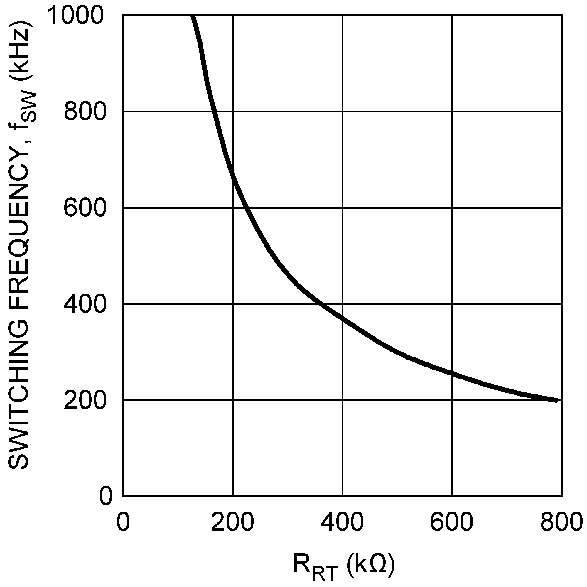 Figure 15. Switching Frequency
The two-channel current regulator of the LM3492/-Q1 is fast response so that it can allow very high contrast ratio (1000:1 at 3-kHz LED dimming frequency, minimum pulse width of the dimming signal is 300 ns). The two channels are dimmable individually. Channel 1 of the current regulator can be disabled by a digital command send through the COMM pin. In this case, the DIM1 pin can serve only as a clock signal for the data flow of the COMM pin. The power dissipated by the current regulator is adaptively minimized by Dynamic Headroom Control to maximize efficiency.
The LM3492/-Q1 can be applied in numerous applications like automotive LCD backlight panels. It can operate efficiently for inputs as high as 65 V. Diagnostic functions including power good indication, overtemperature indication, IOUT overvoltage and undervoltage indications facilitate the interface of the LM3492/-Q1 application circuit with external microprocessors (MCUs). The LM3492/-Q1 will not latch off and continue to operate in the presence of the indications. Other useful features include thermal shutdown, VCC undervoltage lockout, and precision enable. The LM3492/-Q1 is available in the thermally enhanced HTSSOP package.
8.2 Functional Block Diagram
8.3 Feature Description
8.3.1 Switching Frequency
The boost converter of the LM3492/-Q1 device employs a projected-on-time (POT) control method to determine the on-time period of the MOSFET with respect to the input and output voltages and an external resistor RRT. During the on-time period, the boost inductor charges up, and the output capacitor discharges to provide power to the output. A cycle-by-cycle current limit (which is 3.9 A typically and programmable by an external resistor) protects the MOSFET. After the on-time period, the MOSFET turns off and boost inductor discharges. The next on-time period starts when the voltage of the FB pin drops below a threshold which is determined by dynamic headroom control (DHC) and operates from 1.05 V to 2 V. DHC affects the threshold when either the DIM1 pin is high or the DIM2 pin is high.
During POT control operation, the boost converter maintains switching at a nearly constant frequency. During most operating conditions, the switching frequency depends on mainly the value of RRT (Figure 16) but may see some variation with changes in input or output voltage. Also, POT control operation requires no compensation circuit and offers fast transient response of the output voltage. Applications that require very wide input voltage or very wide output voltage ranges may see some variation in the switching frequency as shown in Figure 17 and Figure 18.
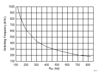
| ILED = 150 mA | VOUT = 30 V | VVIN = 12 V |
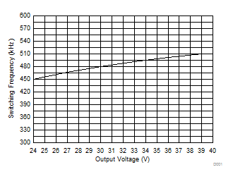
| ILED = 150 mA | RRT = 274 kΩ | VVIN = 12 V | ||
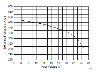
| ILED = 150 mA | VOUT = 30 V | RRT = 274 kΩ |
8.3.2 LDO Regulator
The LM3492/-Q1 device offers an integrated, 5.5-V, LDO regulator. For stability, connect an external capacitor CVCC of more than 0.47-µF between the VCC and GND pins. The current limit of the LDO is typically 30 mA. The LDO regulator can be used to pullup the open-drain COMM pin with an external resistor, and sources current to the ILIM pin to adjust the current limit of the integrated MOSFET. When the voltage on the VCC pin (VCC) is higher than the undervoltage lockout (UVLO) threshold of 3.78 V, the device becomes enabled and the CDHC pin sources a current to charge up an external capacitor (CCDHC) to provide a soft-start function.
8.3.3 Enable and Disable
To enable the LM3492/-Q1 device, the voltage on the EN pin (VEN) must be higher than an enable threshold of typically 1.63 V. If the voltage on the EN pin (VEN) is lower than 1.43 V, the device shuts down. In this case, the LDO regulator turns off and the CDHC pin becomes internally grounded. The EN pin internally pulls up. After enable, a 40-µA current source pulls up the EN pin. If the EN pin is connected to low such that the device is shut down, the pullup current is reduced to 2 µA. These advantages allow the device to effectively avoid false disabling by noise during operation, and minimize power consumption during shutdown. The enable threshold is so precise that it can support a UVLO function for the input voltage as shown in Figure 19. The input voltage can be connected to the EN pin through a resistor divider consisting of REN1 and REN2. This circuitry ensures that the device operates after the input voltage reaches a minimum require value VIN(EN), as shown in Equation 1.
To maintain the VEN level below the absolute maximum specification, place a Zener diode (DEN) between the EN pin and GND pins.
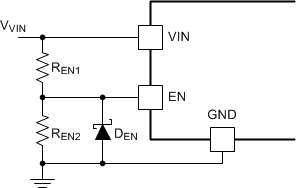 Figure 19. Input Voltage UVLO Implemented by Precision Enable
After the EN pin is pulled low, the device performs the following functions:
- resets IOUT overvoltage and undervoltage indications and the corresponding COMM bit pattern
- resumes the switching frequency tuning to the normal frequency
- resumes channel 1 of the current regulator if it is disabled
Pulling the EN pin low for a short period of approximately 200 ns achieves these same functions with little or no effect on the operation of the boost converter and the current regulator.
8.3.4 Current Limit
The current limit (ICL) of the integrated MOSFET of the LM3492/-Q1 device provides a cycle-by-cycle current limit for protection. This limit can be decreased by injecting a small signal current, IILIM into the ILIM pin. The relationship between ICL and IILIM is described in Equation 2.
where
- ICL(max) is the maximum current limit (3.9 A typical)
As shown in Figure 20, create current limit functionality by connecting a resistor (RILIM) between the VCC pin and the ILIM pin. The typical voltage on the ILIM pin is 0.7 V. To obtain the maximum current limit, connect the ILIM pin to ground.
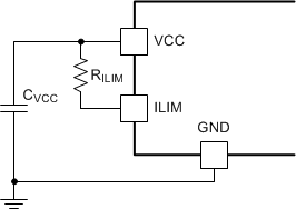 Figure 20. Programmable Current Limit
8.3.5 Thermal Protection
An internal thermal shutdown circuit provides thermal protection. The circuit activates at 165°C (typically) to disable the LM3492/-Q1 device. In this case, the LDO regulator turns off and the CDHC pin becomes internally grounded. Thermal protection helps prevent catastrophic failures from accidental device overheating. When the junction temperature of the device drops below 145°C (typical hysteresis = 20°C), the device resumes normal operation.
8.3.6 Dynamic Headroom Control, Over-Ride, and Soft-Start
The LM3492/-Q1 device uses dynamic headroom control (DHC) to adjust the output voltage (VOUT) of the boost converter to reduce the power loss of the current regulator and thereby maximize efficiency. To understand this control function, consider VLED,n the forward voltage of an LED string connecting to the IOUTn pin and VIOUT,n as the voltage of the IOUTn pin (where n is 1, 2 for channels 1, 2 of the current regulator). VLED,n normally and gradually decreases (in terms of minutes) as a result of the rise of the LED die temperature during operation. The DHC adjusts the output voltage (VOUT) by adjusting a threshold that is reflected in the voltage of the FB pin with reference to VIOUT,n, (the difference between VOUT and VLED,n). The capacitor CCDHC sets the sensitivity of DHC, which affects the response time on adjusting VOUT. If the capacitance value of CCDHC is small, VOUT is more sensitive to the variation of VLED,n.
The CCDHC capacitor acts to control the soft-start functionality. During the start-up period, the voltage of the CDHC pin rises from 0 V to 2.25 V at a rate that depends on the value of the CCDHC capacitor. This limitation ensures that the voltage of the FB pin (as well as the output voltage) ramps up in a controlled manner, and effectively implements a soft-start function.
An internal switch grounds the CDHC pin during any of the following cases:
- VVCC is below the VCC UVLO threshold
- a thermal shutdown occurs
- the EN pin is pulled low
The CDHC pin cannot be connected to the ground externally.
8.3.7 Current Regulator
The LM3492/-Q1 device integrates a two-channel current regulator for controlling the current of two LED strings. The two LED strings dim individually by applying individual dimming signals to the DIM1 and DIM2 pins for LED strings 1 and 2, which are connected from the VOUT pin to the IOUT1 and IOUT2 pins. The device pulls the DIM1 and DIM2 pins low internally. The lowest contrast ratio is 1000:1. The finest pulse width of the dimming signal for the DIM1 and DIM2 pins is 300 ns.
The device sets the current of an LED string (ILED) from 50 mA to 200 mA by using an external resistor RIREF connected between the IREF pin and ground. Figure 21 describes the relationship between ILED and RIREF. The two channels of the current regulator can work in parallel for only one LED string by connecting the IOUT1 and IOUT2 pins together to provide an LED current of up to 400 mA. In this case, connect the DIM1 and DIM2 pins together.
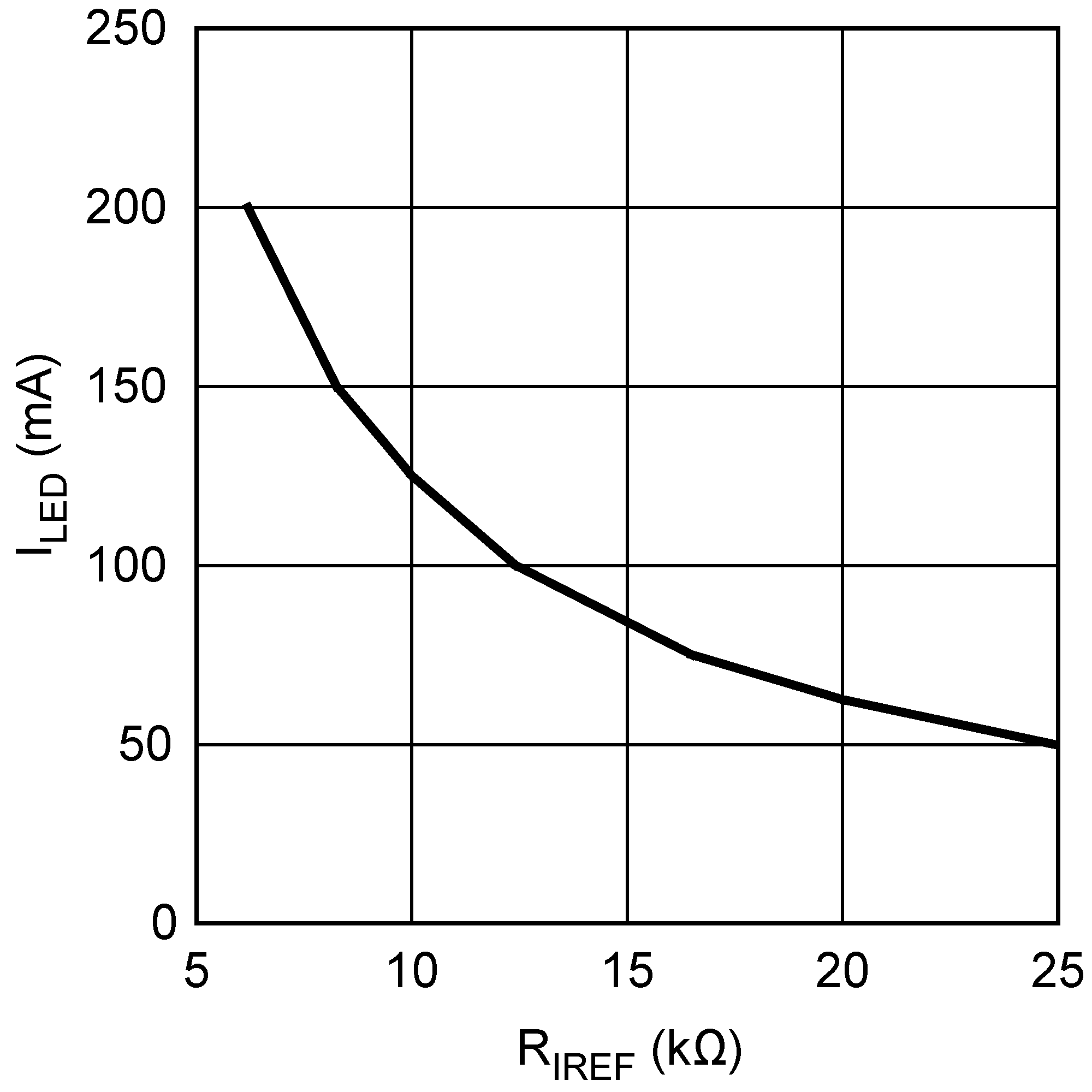 Figure 21. LED Current vs Current Reference Resistance (RIREF)
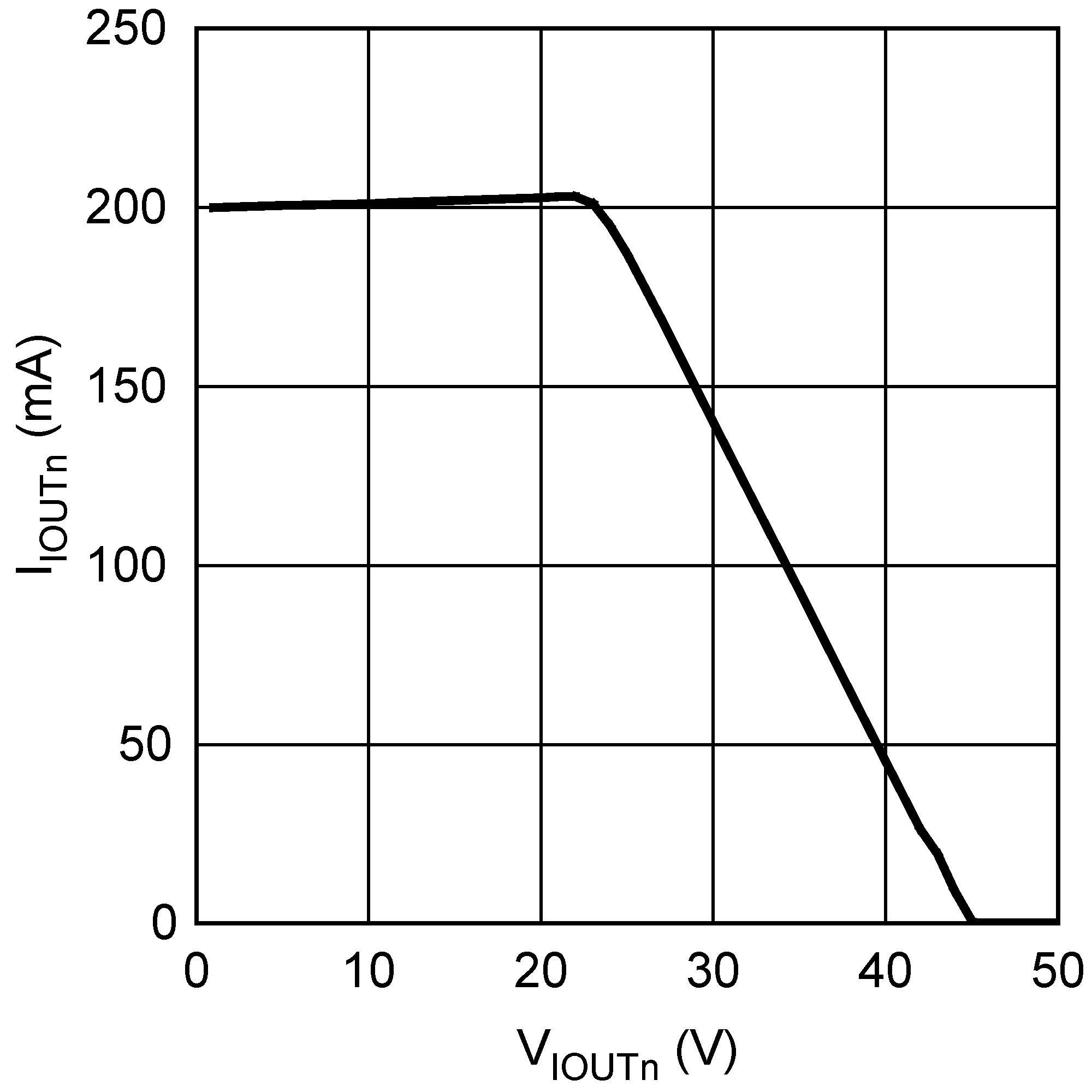 Figure 22. Over-Power Protection
If the voltage on the IOUTn (n = 1, 2) pin is higher than 24 V when channel n is on, the regulated current of channel n reduces linearly if the voltage further increases (as shown in Figure 22). The regulated current of another channel is not affected. This over-power protection feature avoids damaging the current regulator owing to the shorting of many LEDs in one string.
8.3.8 Output Voltage Feedback
The device feeds the output voltage back to the FB pin through a feedback circuit consisting of RFB1, RFB2, and CFB as shown in Figure 23. To assist the feeback functionality, maintain a value of 10 pF for CFB. The DC component of the output voltage feedback uses RFB1 and RFB2. The voltage of the FB pin VFB can be adjusted by DHC. When VFB reaches VFB-OVP, the maximum output voltage of the boost converter VOUT(max) reaches its maximum, as shown in Equation 3.
During DHC operation, maintain the output voltage at a nominal voltage but not the maximum. The nominal output voltage (VOUT(nom)) is described in Equation 4.
where
- VLED,n is the forward voltage of LED string n
- VIOUT,n is the voltage of the IOUTn pin, where n is 1, 2 for channels 1, 2 of the current regulator)
The minimum value of VIOUT,n is approximately 5 Ω × ILED. The nominal voltage of the FB pin (VFB(nom)) is recommended to be from 1.05 V to 2 V. Equation 5 describes the relation between VOUT(max), VOUT(nom), and VFB(nom):
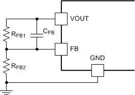 Figure 23. Output Voltage Feedback Circuit
8.3.9 Bidirectional Communication Pin
The COMM pin of the LM3492/-Q1 device is an open-drain bidirectional I/O pin for interfacing with an external MCU for the following functions:
- power-good indication
- overtemperature indication
- output current overvoltage and undervoltage indications
- switching frequency tuning
- channel 1 disabling
Except for the power good indication and the overtemperature alerts, all data flow through the COMM pin is serial and is latched by the falling edge of the signal applying to the DIM1 pin, even when channel 1 of the current regulator is disabled. If the DIM1 pin remains only low or only high, either by an external circuit or by allowing it to open and pull low internally, data does not flow. Figure 24 and Figure 25 show timing diagrams of reading and writing a bit from and to the device through the COMM pin.
Pull up the COMM pin by an MCU I/O pin, which has pullup capability, or an external resistor RCOMM connected to the VCC pin. Without this capability, the voltage of the COMM pin remains at zero. The rise time of the output signal of the COMM pin depends on the pullup power. If the rise time is long (RCOMM is too large or pullup power from the connecting MCU I/O pin is too weak), data may be ready after a longer duration after the falling edge. In this case, the design requires a longer delay between the falling edge latching and the (input or output) bit.
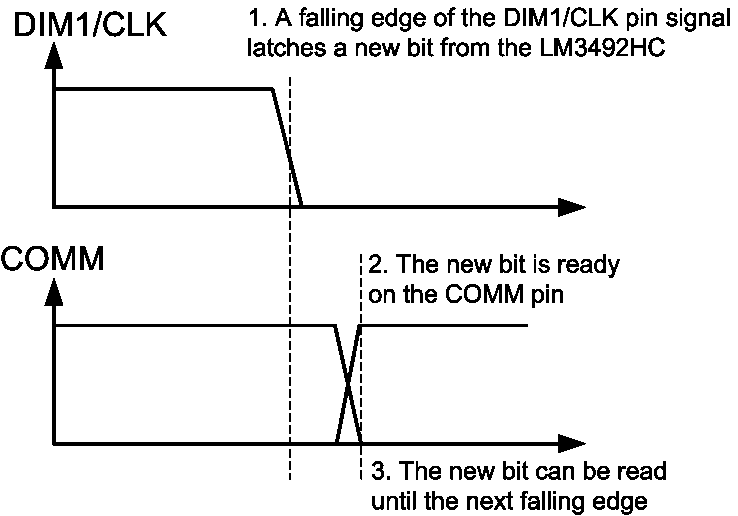 Figure 24. Read from the COMM Pin
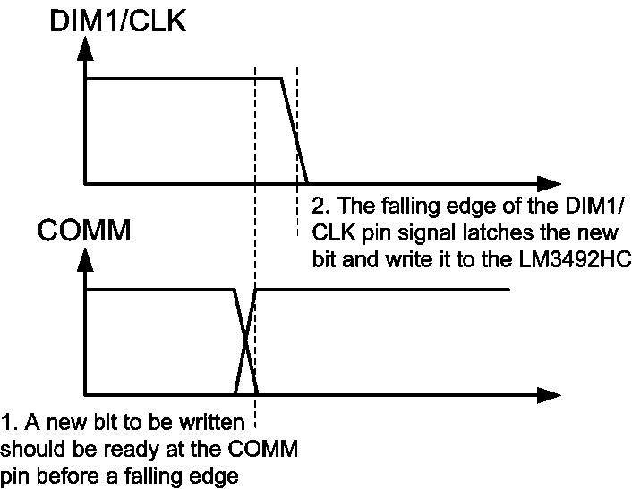 Figure 25. Write to the COMM Pin
8.3.9.1 Power-Good Indication
Upon start-up, the COMM pin reads low. The output voltage of the boost converter of the LM3492/-Q1 device rises until the voltage on the FB pin (VFB) reaches 2.25 V, when the COMM pin reads high to indicate power-good. The power-good indication and the signal applied on the DIM1 pin are independent.
8.3.9.2 Overtemperature Indication
If the junction temperature of the LM3492/-Q1 device reaches 135°C, the COMM pin reads low, showing an overtemperature indication. The external MCU considers to either turn off or reduce the brightness of the LED strings to prevent overtemperature. The overtemperature indication and the signal applied on the DIM1 pin are independent. The COMM pin reads high if the junction temperature falls below 120°C. The device does not latch off and continues to operate in the presence of the overtemperature indication.
8.3.9.3 Output Current Undervoltage Indication
The LM3492/-Q1 device gives an IOUTn (n = 1, 2) undervoltage indication if the voltage of the IOUTn pin when DIMn is high is lower than its minimum required voltage which can regulate ILED, and the voltage of the CDHC pin reaches its maximum. These conditions remain while the device applies 508 consecutive dimming signals on the DIMn pin. This means that the current of the LED string n does not reach the regulation value. In most cases, the IOUT undervoltage indication can be regarded as an open fault of the LED string n. A bit pattern (see Table 1) can be read from the COMM pin. The device does not latch off and continues to operate in the presence of the IOUT undervoltage indication.
8.3.9.4 Switching Frequency Tuning
After power good, the switching frequency (fSW) of the LM3492/-Q1 device can be tuned down 20% or 40%, or resume normal by writing commands (refer to Table 2) to the COMM pin. This functionality helps avoid interfering some sensitive devices, for example radios, working nearby the device. Upon reset, the switching frequency (fSW) of the device resumes normal by default. In the presence of an overtemperature indication or any COMM bit pattern, no command can be written to the device.
8.4 Device Functional Modes
There are no additional functional modes for this device.
8.5 Programming
8.5.1 Output Current Overvoltage Indication
The LM3492/-Q1 device gives an IOUTn (n = 1, 2) overvoltage indication if the voltage of the IOUTn pin when DIMn is higher than a threshold of typically 6.5 V. These conditions remain while the device applies 508 consecutive dimming signals on the DIMn pin. The IOUT overvoltage indication can be regarded as a short fault of the LED string n except the following two cases:
- powering up the device at a very low dimming ratio such that VOUT maintains at a maximum and DHC is not fast enough to reduce VOUT
- during DHC override condition, a bit pattern (see Table 1) can be read from the COMM pin
The device does not latch off and continues to operate in the presence of the IOUT overvoltage indication.
Table 1. COMM Indication Bit Patterns
| CONDITION | PIN | BIT PATTERN |
|---|---|---|
| Overvoltage | IOUT1 | 0001 |
| IOUT2 | 0011 |
|
| Undervoltage | IOUT1 | 0101 |
| IOUT2 | 0111 |
8.5.2 COMM Pin Bit Pattern
Table 1 summarizes all COMM bit patterns of output current overvoltage and undervoltage indications. An existing COMM bit pattern is cleared if one of the following condition occurs:
- the LM3492/-Q1 device is shut down
- the LM3492/-Q1 device is disabled by pulling the EN pin low
- the overtemperature indication is appearing
Apply the clock signal on both DIM1 and DIM2 pins when the COMM bit pattern is read by an external MCU. Before reading the COMM bit pattern, pull the EN pin low for approximately 200 ns to reset the COMM bit pattern. This situation does not affect the operation of the boost converter and the current regulator. After EN is reset, if the IOUT overvoltage or undervoltage condition lasts for 508 consecutive clock cycles, the COMM pin sends the COMM bit pattern for the MCU to read.
In case of overtemperature, the device pulls the COMM pin low to give an overtemperature indication overriding any other pattern. After the overtemperature indication disappears, the COMM bit pattern appears before the overtemperature indication appears again.
8.5.3 Channel 1 Disable
After a power good verification, channel 1 of the current regulator can be disabled by writing a command (see Table 2) to the COMM pin. If LED string 1 is malfunctioning, channel 1 can be disabled and the signal applied on the DIM1 pin can serve as only a clock signal for the data flow of the COMM pin. Channel 1 is by default enabled after reset. If the overtemperature indication or any COMM bit pattern has already presented, no command can be written to the LM3492/-Q1 device.
Table 2. Channel Control Commands
| COMMAND | BIT PATTERN |
|---|---|
| fSW resume normal | 1111 0111 0111 0111 |
| fSW tune down by 20% | 1111 0001 0001 0001 |
| fSW tune down by 40% | 1111 0011 0011 0011 |
| Channel 1 disable | 1111 0101 0101 0101 |