JAJSOT1J December 2008 – June 2022 LM5088 , LM5088-Q1
PRODUCTION DATA
- 1 特長
- 2 アプリケーション
- 3 概要
- 4 Revision History
- 5 Pin Configuration and Functions
- 6 Specifications
-
7 Detailed Description
- 7.1 Overview
- 7.2 Functional Block Diagram
- 7.3
Feature Description
- 7.3.1 High Voltage Low-Dropout Regulator
- 7.3.2 Line Undervoltage Detector
- 7.3.3 Oscillator and Sync Capability
- 7.3.4 Error Amplifier and PWM Comparator
- 7.3.5 Ramp Generator
- 7.3.6 Dropout Voltage Reduction
- 7.3.7 Frequency Dithering (LM5088-1 Only)
- 7.3.8 Cycle-by-Cycle Current Limit
- 7.3.9 Overload Protection Timer (LM5088-2 Only)
- 7.3.10 Soft Start
- 7.3.11 HG Output
- 7.3.12 Thermal Protection
- 7.4 Device Functional Modes
-
8 Application and Implementation
- 8.1 Application Information
- 8.2
Typical Application
- 8.2.1 Design Requirements
- 8.2.2
Detailed Design Procedure
- 8.2.2.1 Timing Resistor
- 8.2.2.2 Output Inductor
- 8.2.2.3 Current Sense Resistor
- 8.2.2.4 Ramp Capacitor
- 8.2.2.5 Output Capacitors
- 8.2.2.6 Input Capacitors
- 8.2.2.7 VCC Capacitor
- 8.2.2.8 Bootstrap Capacitor
- 8.2.2.9 Soft-Start Capacitor
- 8.2.2.10 Output Voltage Divider
- 8.2.2.11 UVLO Divider
- 8.2.2.12 Restart Capacitor (LM5008-2 Only)
- 8.2.2.13 MOSFET Selection
- 8.2.2.14 Diode Selection
- 8.2.2.15 Snubber Components Selection
- 8.2.2.16 Error Amplifier Compensation
- 8.2.3 Application Curves
- 9 Power Supply Recommendations
- 10Layout
- 11Device and Documentation Support
- 12Mechanical, Packaging, and Orderable Information
パッケージ・オプション
メカニカル・データ(パッケージ|ピン)
- PWP|16
サーマルパッド・メカニカル・データ
- PWP|16
発注情報
5 Pin Configuration and Functions
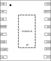
 Figure 5-1 16-PinPWP
Package (Dither Version)(Top
View)
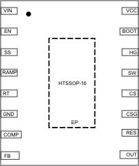
 Figure 5-2 16-PinPWP
Package (Restart Version)
(Top View)
Figure 5-2 16-PinPWP
Package (Restart Version)
(Top View)Table 5-1 Pin Functions
| Pin | Description | Application Information | |
|---|---|---|---|
| Number | Name | ||
| 1 | VIN | Input supply voltage | IC supply voltage. The operating range is 4.5 V to 75 V. |
| 2 | EN | Enable input | If the EN pin voltage is below 0.4 V, the regulator is in a low power state. If the EN pin voltage is between 0.4 V and 1.2 V, the controller is in standby mode. If the EN pin voltage is above 1.2 V, the controller is operational. An external voltage divider can be used to set a line undervoltage shutdown threshold. If the EN pin is left open, a 5-µA pullup current forces the pin to the high state and enables the controller. |
| 3 | SS | Soft start | When SS is below the internal 1.2-V reference, the SS voltage controls the error amplifier. An internal 11-µA current source charges an external capacitor to set the start-up rate of the controller. The SS pin is held low in the standby, VCC UV, and thermal shutdown states. The SS pin can be used for voltage tracking by connecting this pin to a controller voltage supply less than 1.2 V. The applied voltage acts as the reference for the error amplifier. |
| 4 | RAMP | Ramp control signal | An external capacitor connected between this pin and the GND pin sets the ramp slope used for emulated current mode control. The recommended capacitor range 100 pF to 2000 pF. See Section 8 for selection of capacitor value. |
| 5 | RT/SYNC | Internal oscillator frequency set input and synchronization input | The internal oscillator is programmed with a single resistor between this pin and the GND pin. The recommended frequency range is 50 kHz to 1 MHz. An external synchronization signal, which is higher in frequency than the programmed frequency, can be applied to this pin through a small coupling capacitor. The RT resistor to ground is required even when using external synchronization. |
| 6 | GND | Ground | Ground return |
| 7 | COMP | Output of the internal error amplifier | The loop compensation network must be connected between this pin and the FB pin. |
| 8 | FB | Feedback signal from the regulated output | This pin is connected to the inverting input of the internal error amplifier. The regulation threshold is 1.205 V. |
| 9 | OUT | Output voltage connection | Connect this pin directly to the regulated output voltage. |
| 10 | DITH | Frequency Dithering (LM5088-1 Only) | A capacitor connected between DITH pin and GND is charged and discharged by 27-µA current sources. As the voltage on the DITH pin ramps up and down, the oscillator frequency is modulated between –5% to +5% of the nominal frequency set by the RT resistor. Grounding the DITH pin disables the frequency dithering mode. |
| 10 | RES | Hiccup Mode Restart (LM5088-2 Only) | The RES pin is normally connected to an external capacitor that sets the timing for hiccup mode current limiting. In normal operation, a 25-µA current source discharges the RES pin capacitor to ground. If cycle-by-cycle current limit threshold is exceeded during any PWM cycle, the current sink is disabled and RES capacitor is charged by an internal 50-µA current. If the RES voltage reaches 1.2 V, the HG pin gate drive signal is disabled and the RES pin capacitor is discharged by a 1-µA current sink. Normal operation resumes when the RES pin falls below 0.2 V. |
| 11 | CSG | Current Sense Ground | Low-side reference for the current sense resistor |
| 12 | CS | Current sense | Current measurement connection for the re-circulating diode. An external sense resistor and an internal sample and hold circuit sense the diode current at the conclusion of the buck switch off time. This current measurement provides the DC offset level for the emulated current ramp. |
| 13 | SW | Switching node | Connect this pin to the source terminal of the external MOSFET switch. |
| 14 | HG | High gate | Connect this pin to the gate terminal of the external MOSFET switch. |
| 15 | BOOT | Input for bootstrap capacitor | An external capacitor is required between the BOOT and the SW pins to provide bias to the MOSFET gate driver. The capacitor is charged from VCC via an internal diode during the off-time of the buck switch. |
| 16 | VCC | Output of the bias regulator | VCC tracks VIN up to the regulation level (7.8 V typical). A 0.1-µF to 10-µF ceramic decoupling capacitor is required. An external voltage between 8.3 V and 13 V can be applied to this pin to reduce internal power dissipation. |
| 17 | EP | Exposed pad | Exposed pad of the package. Electrically isolated. Must be soldered to the ground plane to reduce thermal resistance. |