JAJSI34H February   2019  – June 2024 LM63615-Q1 , LM63625-Q1

PRODUCTION DATA  

  1.   1
  2. 特長
  3. アプリケーション
  4. 概要
  5. Device Comparison Table
  6. Pin Configuration and Functions
  7. Specifications
    1.     Absolute Maximum Ratings
    2. 6.1 ESD Ratings
    3. 6.2 Recommended Operating Conditions
    4. 6.3 Thermal Information
    5. 6.4 Electrical Characteristics
    6. 6.5 Timing Characteristics
    7. 6.6 Switching Characteristics
    8. 6.7 System Characteristics
    9. 6.8 Typical Characteristics
  8. Detailed Description
    1. 7.1 Overview
    2. 7.2 Functional Block Diagram
    3. 7.3 Feature Description
      1. 7.3.1 Sync/Mode Selection
      2. 7.3.2 Output Voltage Selection
      3. 7.3.3 Switching Frequency Selection
        1. 7.3.3.1 Spread Spectrum Option
      4. 7.3.4 Enable and Start-Up
      5. 7.3.5 RESET Flag Output
      6. 7.3.6 Undervoltage Lockout and Thermal Shutdown and Output Discharge
    4. 7.4 Device Functional Modes
      1. 7.4.1 Overview
      2. 7.4.2 Light Load Operation
        1. 7.4.2.1 Sync/FPWM Operation
      3. 7.4.3 Dropout Operation
      4. 7.4.4 Minimum On-time Operation
      5. 7.4.5 Current Limit and Short-Circuit Operation
  9. Application and Implementation
    1. 8.1 Application Information
    2. 8.2 Typical Application
      1. 8.2.1 Design Requirements
      2. 8.2.2 Detailed Design Procedure
        1. 8.2.2.1 Choosing the Switching Frequency
        2. 8.2.2.2 Setting the Output Voltage
          1. 8.2.2.2.1 CFF Selection
        3. 8.2.2.3 Inductor Selection
        4. 8.2.2.4 Output Capacitor Selection
        5. 8.2.2.5 Input Capacitor Selection
        6. 8.2.2.6 CBOOT
        7. 8.2.2.7 VCC
        8. 8.2.2.8 External UVLO
        9. 8.2.2.9 Maximum Ambient Temperature
      3. 8.2.3 Full Feature Design Example
      4. 8.2.4 Application Curves
      5. 8.2.5 EMI Performance Curves
    3. 8.3 Best Design Practices
    4. 8.4 Power Supply Recommendations
    5. 8.5 Layout
      1. 8.5.1 Layout Guidelines
        1. 8.5.1.1 Ground and Thermal Considerations
      2. 8.5.2 Layout Example
  10. Device and Documentation Support
    1. 9.1 Device Support
      1. 9.1.1 Device Nomenclature
    2. 9.2 Documentation Support
      1. 9.2.1 Related Documentation
    3. 9.3 ドキュメントの更新通知を受け取る方法
    4. 9.4 サポート・リソース
    5. 9.5 Trademarks
    6. 9.6 静電気放電に関する注意事項
    7. 9.7 用語集
  11. 10Revision History
  12. 11Mechanical, Packaging, and Orderable Information

パッケージ・オプション

メカニカル・データ(パッケージ|ピン)
サーマルパッド・メカニカル・データ
発注情報

EMI Performance Curves

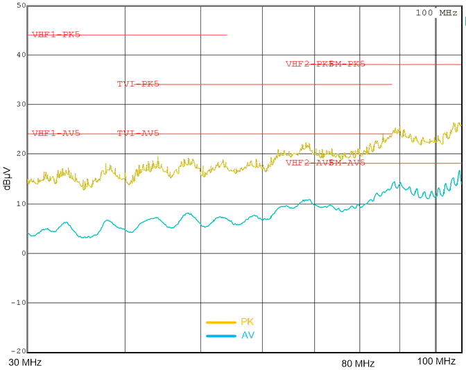
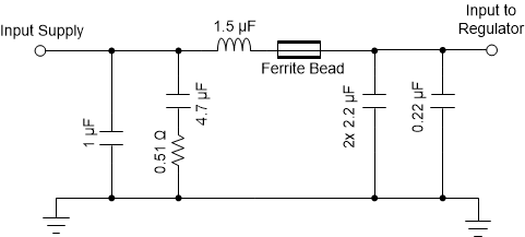
EMI results critically depend on PCB layout and test setup. The results given here are typical and given for information purposes only. Figure 8-45 shows the used EMI filter. The limit lines shown refer to CISPR25 class 5.
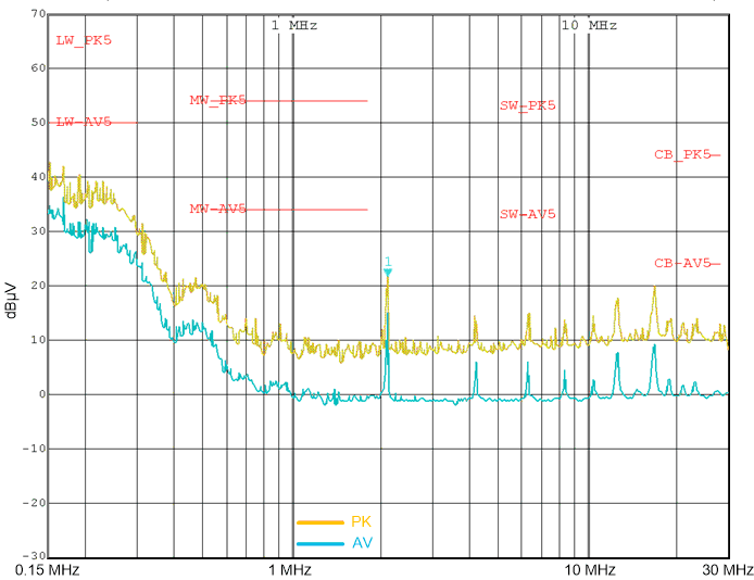
LM63615-Q1 LM63625-Q1 Typical Conducted EMI  0.15 MHz to 30 MHz
LM63625DQVOUT = 5 VƒSW = 2100 kHz
IOUT = 2.5 ADither
Figure 8-45 Typical Conducted EMI 0.15 MHz to 30 MHz
LM63615-Q1 LM63625-Q1 Typical Conducted EMI 30 MHz to 108 MHz
LM63625DQVOUT = 5 VƒSW = 2100 kHz
IOUT = 2.5 ADither
Figure 8-46 Typical Conducted EMI 30 MHz to 108 MHz
LM63615-Q1 LM63625-Q1 Typical Input EMI Filter
Input filter used only for EMI measurements shown in the Section 8.2.5 section.
Figure 8-47 Typical Input EMI Filter