JAJSPI9H June   2011  – November 2024 LP2951-Q1

PRODUCTION DATA  

  1.   1
  2. 特長
  3. アプリケーション
  4. 概要
  5. Pin Configuration and Functions
  6. Specifications
    1. 5.1 Absolute Maximum Ratings
    2. 5.2 ESD Ratings
    3. 5.3 Recommended Operating Conditions
    4. 5.4 Thermal Information
    5. 5.5 Electrical Characteristics (Both Legacy and New Chip)
    6. 5.6 Timing Requirements (New Chip only)
    7. 5.7 Typical Characteristics
  7. Detailed Description
    1. 6.1 Overview
    2. 6.2 Functional Block Diagram
    3. 6.3 Feature Description
      1. 6.3.1 Output Enable
      2. 6.3.2 Dropout Voltage
      3. 6.3.3 Current Limit
      4. 6.3.4 Undervoltage Lockout (UVLO)
      5. 6.3.5 Thermal Shutdown
    4. 6.4 Device Functional Modes
      1. 6.4.1 Shutdown Mode
  8. Application and Implementation
    1. 7.1 Application Information
      1. 7.1.1 Reverse Current
      2. 7.1.2 Input and Output Capacitor Requirements
      3. 7.1.3 Estimating Junction Temperature
      4. 7.1.4 Power Dissipation (PD)
    2. 7.2 Typical Application
      1. 7.2.1 Design Requirements
        1. 7.2.1.1 Recommended Capacitor Types
          1. 7.2.1.1.1 Recommended Capacitors (Legacy Chip)
            1. 7.2.1.1.1.1 ESR Range (Legacy Chip)
          2. 7.2.1.1.2 Recommended Capacitors (New Chip)
      2. 7.2.2 Detailed Design Procedure
        1. 7.2.2.1 Feedback Resistor Selection
        2. 7.2.2.2 Feedforward Capacitor
      3. 7.2.3 Application Curves
    3. 7.3 Power Supply Recommendations
    4. 7.4 Layout
      1. 7.4.1 Layout Guidelines
      2. 7.4.2 Layout Example
  9. Device and Documentation Support
    1. 8.1 Device Support
      1. 8.1.1 Development Support
      2. 8.1.2 Device Nomenclature
    2. 8.2 Documentation Support
      1. 8.2.1 Related Documentation
    3. 8.3 ドキュメントの更新通知を受け取る方法
    4. 8.4 サポート・リソース
    5. 8.5 Trademarks
    6. 8.6 静電気放電に関する注意事項
    7. 8.7 用語集
  10. Revision History
  11. 10Mechanical, Packaging, and Orderable Information

パッケージ・オプション

メカニカル・データ(パッケージ|ピン)
サーマルパッド・メカニカル・データ
発注情報

Current Limit

The device has an internal current limit circuit that protects the regulator during transient high-load current faults or shorting events. The current limit is a brick-wall scheme. In a high-load current fault, the brick-wall scheme limits the output current to the current limit (ICL). ICL is listed in the 電気的特性 table.

The output voltage is not regulated when the device is in current limit. When a current limit event occurs, the device begins to heat up because of the increase in power dissipation. When the device is in brick-wall current limit, the pass transistor dissipates power [(VIN – VOUT) × ICL]. If thermal shutdown is triggered, the device turns off. After the device cools down, the internal thermal shutdown circuit turns the device back on. If the output current fault condition continues, the device cycles between current limit and thermal shutdown. For more information on current limits, see the Know Your Limits application note.

Figure 6-1 shows a diagram of the current limit.
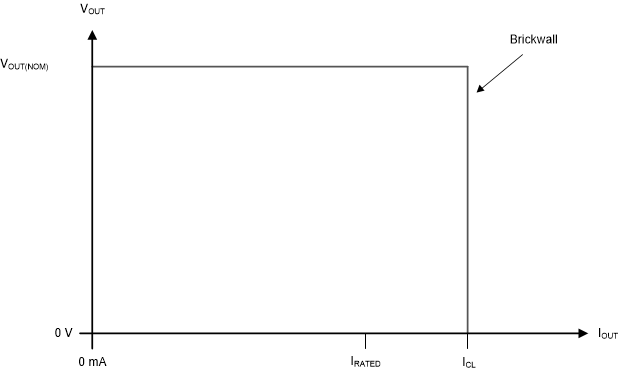
LP2951-Q1 Current
                    Limit Figure 6-1 Current Limit