SNVS095F May 2004 – March 2015 LP2952-N , LP2953
PRODUCTION DATA.
- 1 Features
- 2 Applications
- 3 Description
- 4 Revision History
- 5 Pin Configuration and Functions
- 6 Specifications
- 7 Detailed Description
-
8 Application and Implementation
- 8.1 Application Information
- 8.2
Typical Applications
- 8.2.1 Basic 5-V Regulator
- 8.2.2 5-V Current Limiter with Load Fault Indicator
- 8.2.3 Low Temperature Coefficient Current Sink
- 8.2.4 5-V Regulator With Error Flags for Low Battery and Out of Regulation
- 8.2.5 5-V Battery Powered Supply With Backup and Low Battery Flag
- 8.2.6 5-V Regulator With Timed Power-On Reset
- 8.2.7 5-V Regulator With Snap-ON and Snap-OFF Features and Hysteresis
- 8.2.8 5-V Regulator With Error Flags for Low Battery and Out of Regulation With Snap-ON or Snap-OFF Output
- 8.2.9 5-V Regulator With Timed Power-On Reset, Snap-ON and Snap-OFF Features, and Hysteresis
- 9 Power Supply Recommendations
- 10Layout
- 11Device and Documentation Support
- 12Mechanical, Packaging, and Orderable Information
8 Application and Implementation
NOTE
Information in the following applications sections is not part of the TI component specification, and TI does not warrant its accuracy or completeness. TI’s customers are responsible for determining suitability of components for their purposes. Customers should validate and test their design implementation to confirm system functionality.
8.1 Application Information
 Figure 30. Schematic Diagram
8.1.1 External Capacitors
A 2.2-μF (or greater) capacitor is required between the OUT pin and ground to assure stability when the output is set to 5 V. Without this capacitor, the device will oscillate. Most types of tantalum or aluminum electrolytic capacitors will work here. Film types will work, but are more expensive. Many aluminum electrolytic capacitors contain electrolytes which freeze at −30°C, which requires the use of solid tantalum capacitors below −25°C. The important parameters of the capacitor are an equivalent series resistance (ESR) of about 5 Ω or less and a resonant frequency above 500 kHz (the ESR may increase by a factor of 20 or 30 as the temperature is reduced from 25°C to −30°C). The value of this capacitor may be increased without limit.
At lower values of output current, less output capacitance is required for stability. The capacitor can be reduced to 0.68 μF for currents below 10 mA or 0.22 μF for currents below 1 mA.
Programming the output for voltages below 5 V runs the error amplifier at lower gains requiring more output capacitance for stability. At 3.3-V output, a minimum of 4.7 μF is required. For the worst-case condition of 1.23-V output and 250 mA of load current, a 6.8-μF (or larger) capacitor should be used.
A 1-μF capacitor should be placed from the IN pin to ground if there is more than 10 inches of wire between the IN pin and the ac filter capacitor or if a battery input is used.
Stray capacitance to the FEEDBACK pin can cause instability. This problem is most likely to appear when using high-value external resistors to set the output voltage. Adding a 100-pF capacitor between the OUT and FEEDBACK pins and increasing the output capacitance to 6.8 μF (or greater) will cure the problem.
8.1.2 Minimum Load
When setting the output voltage using an external resistive divider, a minimum current of 1 μA is recommended through the resistors to provide a minimum load.
It should be noted that a minimum load current is specified in several of the Electrical Characteristics: All Voltage Options test conditions, so this value must be used to obtain correlation on these tested limits.
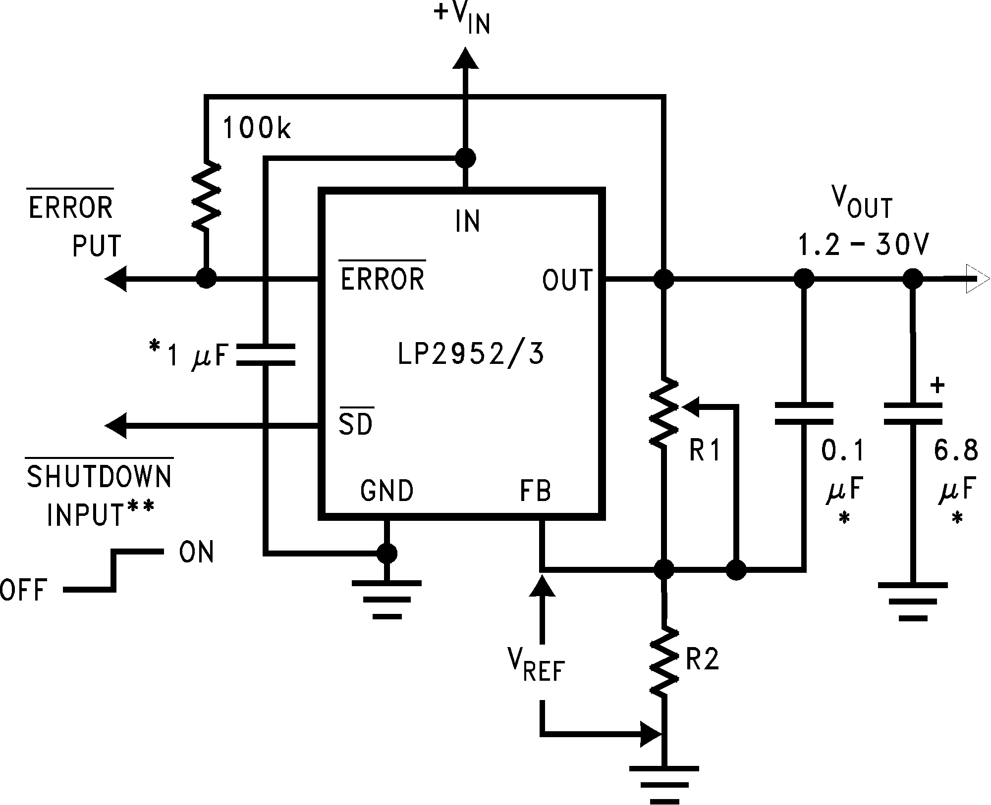
8.1.3 Programming the Output Voltage
The regulator may be pin-strapped for 5-V operation using its internal resistive divider by tying the OUTPUT and SENSE pins together and also tying the FEEDBACK and VTAP pins together.
Alternatively, it may be programmed for any voltage between the 1.23-V reference and the 30-V maximum rating using an external pair of resistors (see Figure 31). The complete equation for the output voltage is:

where
- VREF is the 1.23-V reference and IFB is the FEEDBACK pin bias current (−20 nA, typical).
The minimum recommended load current of 1 μA sets an upper limit of 1.2 MΩ on the value of R2 in cases where the regulator must work with no load (see Minimum Load). IFB will produce a typical 2% error in VOUT which can be eliminated at room temperature by trimming R1. For better accuracy, choosing R2 = 100 kΩ will reduce this error to 0.17% while increasing the resistor program current to 12 μA. Because the typical quiescent current is 120 μA, this added current is negligible.

** Drive with TTL-low to shutdown
8.1.4 Dropout Voltage
The dropout voltage of the regulator is defined as the minimum input-to-output voltage differential required for the output voltage to stay within 100 mV of the output voltage measured with a 1-V differential. The dropout voltage is independent of the programmed output voltage.
8.1.5 Dropout Detection Comparator
This comparator produces a logic low whenever the output falls out of regulation by more than about 5%. This value results from the comparator built-in offset of 60 mV divided by the 1.23-V reference (see Functional Block Diagrams). The 5% low trip level remains constant regardless of the programmed output voltage. An out-of-regulation condition can result from low input voltage, current limiting, or thermal limiting.
Figure 32 gives a timing diagram showing the relationship between the output voltage, the ERROR output, and input voltage as the input voltage is ramped up and down to a regulator programmed for 5-V output. The ERROR signal becomes low at about 1.3-V input. It goes high at about 5-V input, where the output equals 4.75 V. Because the dropout voltage is load dependent, the input voltage trip points will vary with load current. The output voltage trip point does not vary.
The comparator has an open-collector output which requires an external pullup resistor. This resistor may be connected to the regulator output or some other supply voltage. Using the regulator output prevents an invalid high on the comparator output that occurs if it is pulled up to an external voltage while the regulator input voltage is reduced below 1.3 V. In selecting a value for the pullup resistor, note that while the output can sink 400 μA, this current adds to battery drain. Suggested values range from 100 kΩ to 1 MΩ. This resistor is not required if the output is unused.
When VIN ≤ 1.3 V, the ERROR pin becomes a high impedance, allowing the error flag voltage to rise to its pullup voltage. Using VOUT as the pullup voltage (rather than an external 5-V source) will keep the error flag voltage below 1.2 V (typical) in this condition. The user may wish to divide down the error flag voltage using equal-value resistors (10 kΩ is suggested) to ensure a low-level logic signal during any fault condition, while still allowing a valid logic high level during normal operation.

** Exact value depends on dropout voltage. (See Power Supply Recommendations)
8.1.6 Output Isolation
The regulator output can be left connected to an active voltage source (such as a battery) with the regulator input power shut off, as long as the regulator ground pin is connected to ground. If the ground pin is left floating, damage to the regulator can occur if the output is pulled up by an external voltage source. If the regulator input power (VIN) is applied, and the SHUTDOWN pin is low, the automatic output discharge circuit will be active, and any voltage source applied to the output will be discharged to ground.
8.1.7 Reducing Output Noise
In reference applications it may be advantageous to reduce the ac noise present on the output. One method is to reduce regulator bandwidth by increasing output capacitance. This is relatively inefficient, because large increases in capacitance are required to get significant improvement.
Noise can be reduced more effectively by a bypass capacitor placed across R1 (see Figure 31). The formula for selecting the capacitor to be used is:

This gives a value of about 0.1 μF. When this is used, the output capacitor must be 6.8 μF (or greater) to maintain stability. The 0.1-μF capacitor reduces the high-frequency gain of the circuit to unity, lowering the output noise from 260 μV to 80 μV using a 10-Hz to 100-kHz bandwidth. Also, noise is no longer proportional to the output voltage, so improvements are more pronounced at high output voltages.
8.1.8 Auxiliary Comparator (LP2953 Only)
The LP2953 contains an auxiliary comparator whose inverting input is connected to the 1.23-V reference. The auxiliary comparator has an open-collector output whose electrical characteristics are similar to the dropout detection comparator. The noninverting input and output are brought out for external connections.
8.1.9 SHUTDOWN Input
A logic-level signal will shut off the regulator output when a low (< 1.2 V) is applied to the SHUTDOWN input.
To prevent possible mis-operation, the SHUTDOWN input must be actively terminated. If the input is driven from open-collector logic, a pullup resistor (20 kΩ to 100 kΩ is recommended) should be connected from the SHUTDOWN input to the regulator input.
If the SHUTDOWN input is driven from a source that actively pulls high and low (like an op-amp), the pullup resistor is not required, but may be used.
If the shutdown function is not to be used, the cost of the pullup resistor can be saved by simply tying the SHUTDOWN input directly to the regulator input.
NOTE
Because the Absolute Maximum Ratings state that the SHUTDOWN input can not go more than 0.3 V below ground, the reverse battery-input protection feature which protects the regulator input is sacrificed if the SHUTDOWN input is tied directly to the regulator input.
If reverse-battery input protection is required in an application, the pullup resistor between the SHUTDOWN input and the regulator input must be used.
8.2 Typical Applications
8.2.1 Basic 5-V Regulator
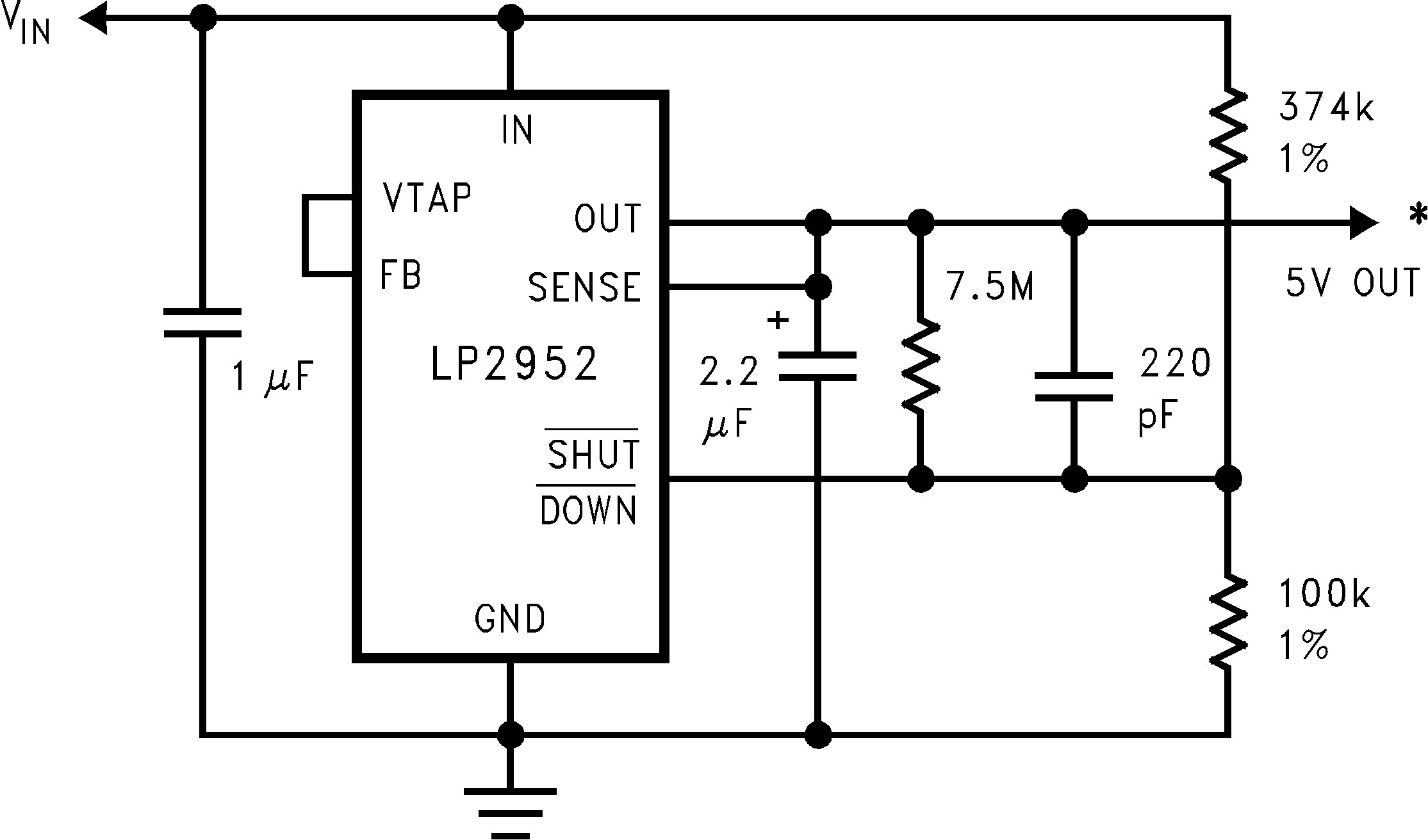
 Figure 33. Basic 5-V Regulator
8.2.1.1 Design Requirements
For this design example, use the parameters listed in Table 1 as the input parameters.
Table 1. Design Parameters
| DESIGN PARAMETER | DESIGN REQUIREMENT |
|---|---|
| Input voltage | 6 V, ±10%, provided by the DC-DC converter switching at 1 MHz |
| Output voltage | 5 V, ±1% |
| Output current | 250 mA (maximum), 1 mA (minimum) |
| RMS noise, 10 Hz to 100 kHz | 1 mV typical |
| PSRR at 1 kHz | 50 dB typical |
8.2.1.2 Detailed Design Procedure
At 150-mA loading, the dropout of the LP2952 and LP2953 has 600-mV maximum dropout over temperature — thus, a 1500-mV headroom is sufficient for operation over both input and output voltage accuracy. The efficiency of the LP2952 and LP2953 in this configuration is VOUT / VIN = 83.3%. Input and output capacitors are selected in accordance with the External Capacitors section. Ceramic capacitances of 1 μF for the input and one 2.2-μF capacitor for the output are selected. With an efficiency of 83.3% and a 250-mA maximum load, the internal power dissipation is 250 mW, which corresponds to a 19.2°C junction temperature rise for the SOIC package. With a VIN – VOUT differential of 1 V and a maximum load current of 250 mA the internal junction temperature (TJ) of the SOIC package will rise 19.2°C above the ambient temperature. With an 85°C maximum ambient temperature, the junction temperature is at 104.2°C. To minimize noise, a bypass capacitor of 100 pF is selected between OUT and FEEDBACK pins.
8.2.1.3 Application Curves
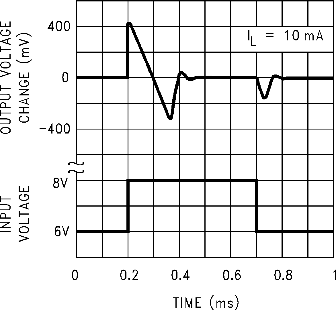
 Figure 34. Line Transient Response
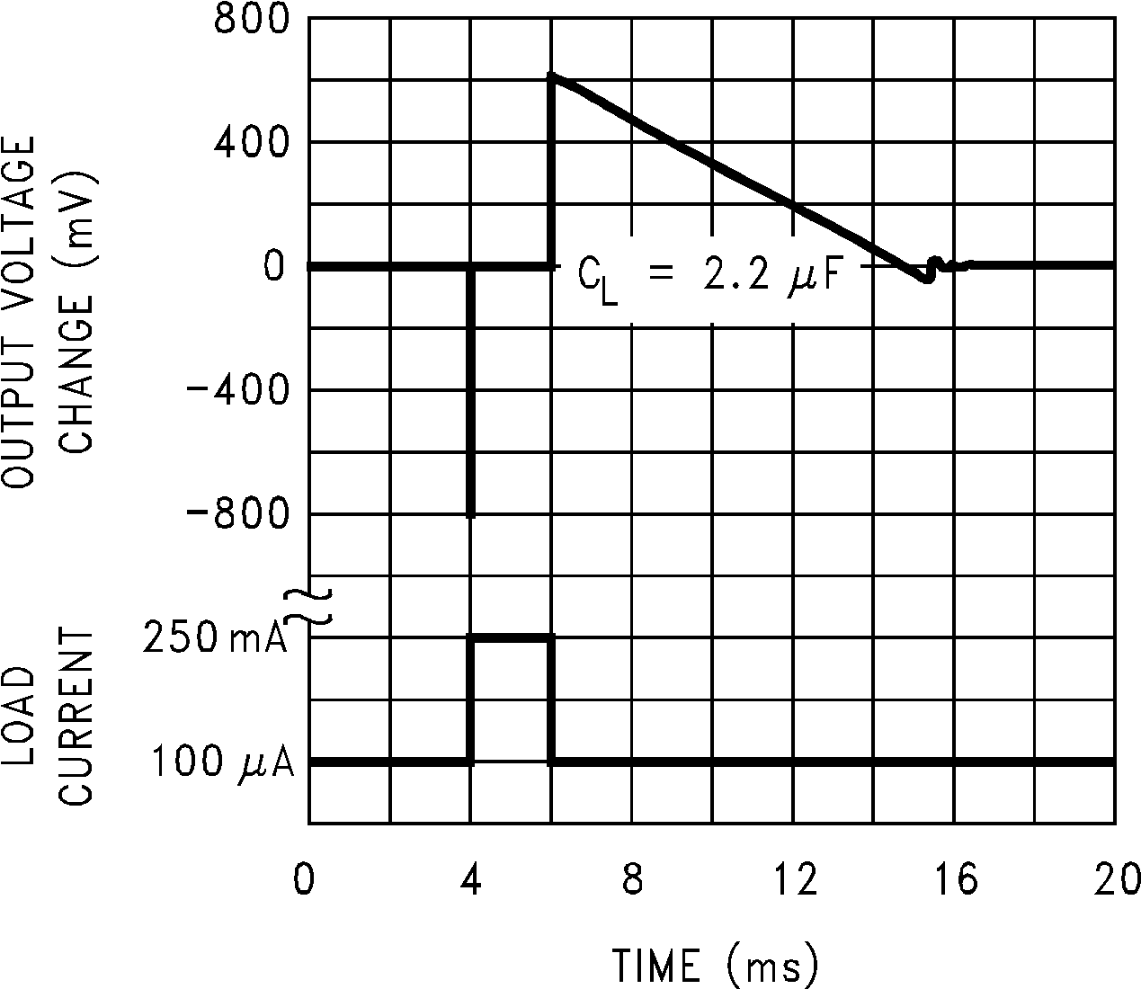
 Figure 35. Load Transient Response
8.2.2 5-V Current Limiter with Load Fault Indicator
Figure 36 is the example circuit for 5-V current limiter with load fault indicator, it has the following features:
- Output voltage equals +VIN minimum dropout voltage, which varies with output current. Current limits at a maximum of 380 mA (typical).
- Select R1 so that the comparator input voltage is 1.23 V at the output voltage which corresponds to the desired fault current value.
 Figure 36. 5-V Current Limiter With Load Fault Indicator
8.2.3 Low Temperature Coefficient Current Sink
The LP2952 or LP2953 can be used as a low drift current source as Figure 37 shows. By connecting VOUT to FEEDBACK, VOUT will be regulated at 1.235 V, and current consumption at R is IOUT = 1.23/R.
 Figure 37. Low Temperature Coefficient Current Sink
8.2.4 5-V Regulator With Error Flags for Low Battery and Out of Regulation
Figure 38 is the example circuit for 5-V regulator with error flags for low battery and out of regulation, it has the following features:
- Connect to logic or microprocessor control inputs.
- LOW BATT flag warns the user that the battery has discharged down to about 5.8 V, giving the user time to recharge the battery or power down some hardware with high power requirements. The output is still in regulation at this time.
- OUT OF REGULATION flag indicates when the battery is almost completely discharged, and can be used to initiate a power-down sequence.
 Figure 38. 5-V Regulator With Error Flags for Low Battery and Out of Regulation
8.2.5 5-V Battery Powered Supply With Backup and Low Battery Flag
Figure 39 is the example circuit for 5-V battery powered supply with backup and low battery flag, it has the following features:
- The circuit switches to the NI-CAD backup battery when the main battery voltage drops below about 5.6 V and returns to the main battery when its voltage is recharged to about 6 V.
- The 5-V MAIN output powers circuitry which requires no backup, and the 5-V MEMORY output powers critical circuitry which cannot be allowed to lose power.
- The BATTERY LOW flag goes low whenever the circuit switches to the NI-CAD backup battery.
 Figure 39. 5-V Battery Powered Supply With Backup and Low Battery Flag
8.2.6 5-V Regulator With Timed Power-On Reset
Figure 40 is the circuit designed to generate a adjustable power on reset signal. Adjusting RT and CT values causes a certain delay time as Figure 41 shows.
 Figure 40. 5-V Regulator With Timed Power-On Reset

8.2.7 5-V Regulator With Snap-ON and Snap-OFF Features and Hysteresis
Figure 42 is the circuit designed to generate 5-V regulator with snap-ON and snap-OFF features and hysteresis. The output turns on at VIN = 5.87 V and turns off at VIN = 5.64 V.

Turns off at VIN = 5.64 V
(for component values shown)
8.2.8 5-V Regulator With Error Flags for Low Battery and Out of Regulation With Snap-ON or Snap-OFF Output
Figure 43 is the circuit as 5-V regulator with error flags for low battery and out of regulation with Snap-ON/Snap-OFF output. It has the following features:
- Connect to logic or microprocessor control inputs.
- LOW BATT flag warns the user that the battery has discharged down to about 5.8 V, giving the user time to recharge the battery or shutdown hardware with high power requirements. The output is still in regulation at this time.
- OUT OF REGULATION flag goes low if the output goes below about 4.7 V, which could occur from a load fault.
- OUTPUT has Snap-ON or Snap-OFF feature. Regulator snaps ON at about 5.7-V input, and OFF at about 5.6 V.
 Figure 43. 5-V Regulator With Error Flags for Low Battery and Out of Regulation With Snap-ON or Snap-OFF Output
8.2.9 5-V Regulator With Timed Power-On Reset, Snap-ON and Snap-OFF Features, and Hysteresis
Figure 44 is the circuit designed for 5-V regulator with timed power-on reset, Snap-ON and Snap-OFF features, and hysteresis. Its timing diagram shows as Figure 45.
 Figure 44. 5-V Regulator With Timed Power-On Reset, Snap-ON or Snap-OFF Feature, and Hysteresis
