SNVS095F May 2004 – March 2015 LP2952-N , LP2953
PRODUCTION DATA.
- 1 Features
- 2 Applications
- 3 Description
- 4 Revision History
- 5 Pin Configuration and Functions
- 6 Specifications
- 7 Detailed Description
-
8 Application and Implementation
- 8.1 Application Information
- 8.2
Typical Applications
- 8.2.1 Basic 5-V Regulator
- 8.2.2 5-V Current Limiter with Load Fault Indicator
- 8.2.3 Low Temperature Coefficient Current Sink
- 8.2.4 5-V Regulator With Error Flags for Low Battery and Out of Regulation
- 8.2.5 5-V Battery Powered Supply With Backup and Low Battery Flag
- 8.2.6 5-V Regulator With Timed Power-On Reset
- 8.2.7 5-V Regulator With Snap-ON and Snap-OFF Features and Hysteresis
- 8.2.8 5-V Regulator With Error Flags for Low Battery and Out of Regulation With Snap-ON or Snap-OFF Output
- 8.2.9 5-V Regulator With Timed Power-On Reset, Snap-ON and Snap-OFF Features, and Hysteresis
- 9 Power Supply Recommendations
- 10Layout
- 11Device and Documentation Support
- 12Mechanical, Packaging, and Orderable Information
6 Specifications
6.1 Absolute Maximum Ratings
over operating free-air temperature range (unless otherwise noted)(1)| MIN | MAX | UNIT | |
|---|---|---|---|
| Power dissipation(2) | Internally Limited | ||
| Input supply voltage | −20 | 30 | V |
| FEEDBACK input voltage(3) | −0.3 | 5 | V |
| Comparator input voltage(4) | −0.3 | 30 | V |
| SHUTDOWN input voltage(4) | −0.3 | 30 | V |
| Comparator output voltage(4) | −0.3 | 30 | V |
| Maximum junction temperature | 150 | °C | |
| Storage temperature, Tstg | −65 | 150 | °C |
(1) Stresses beyond those listed under Absolute Maximum Ratings may cause permanent damage to the device. These are stress ratings only, which do not imply functional operation of the device at these or any other conditions beyond those indicated under Recommended Operating Conditions. Exposure to absolute-maximum-rated conditions for extended periods may affect device reliability.
(2) The maximum allowable power dissipation is a function of the maximum junction temperature, TJ(MAX), the junction-to-ambient thermal resistance, RθJA, and the ambient temperature, TA. The maximum allowable power dissipation at any ambient temperature is calculated using the equation for P(MAX): P(MAX) = (TJ(MAX) – TA) / RθJA.
Exceeding the maximum allowable power dissipation will cause excessive die temperature, and the regulator will go into thermal shutdown. See Power Supply Recommendations for additional information on heatsinking and thermal resistance.
Exceeding the maximum allowable power dissipation will cause excessive die temperature, and the regulator will go into thermal shutdown. See Power Supply Recommendations for additional information on heatsinking and thermal resistance.
(3) When used in dual-supply systems where the regulator load is returned to a negative supply, the output voltage must be diode-clamped to ground.
(4) May exceed the input supply voltage.
6.2 ESD Ratings
| VALUE | UNIT | |||
|---|---|---|---|---|
| V(ESD) | Electrostatic discharge | Human body model (HBM), per ANSI/ESDA/JEDEC JS-001, all pins(1) | ±2000 | V |
(1) JEDEC document JEP155 states that 500-V HBM allows safe manufacturing with a standard ESD control process.
6.3 Recommended Operating Conditions
over operating free-air temperature range (unless otherwise noted)| MIN | MAX | UNIT | ||
|---|---|---|---|---|
| Operating junction temperature | −40 | 125 | °C | |
| Input supply voltage | 2.3 | 30 | V | |
6.4 Thermal Information
| THERMAL METRIC(1) | LP2952, LP2953 | LP2953 | UNIT | |
|---|---|---|---|---|
| SOIC (D) | PDIP (NBG) | |||
| 16 PINS | ||||
| RθJA | Junction-to-ambient thermal resistance | 76.9 | 42.1 | °C/W |
| RθJC(top) | Junction-to-case (top) thermal resistance | 37.4 | 28.1 | |
| RθJB | Junction-to-board thermal resistance | 34.6 | 22.2 | |
| ψJT | Junction-to-top characterization parameter | 7.3 | 12.0 | |
| ψJB | Junction-to-board characterization parameter | 34.3 | 22.1 | |
(1) For more information about traditional and new thermal metrics, see the IC Package Thermal Metrics application report, SPRA953.
6.5 Electrical Characteristics: 3.3-V Versions
Limits are assured by production testing or correlation techniques using standard Statistical Quality Control (SQC) methods. Unless otherwise specified: MIN (minimum) and MAX (maximum) specifications in apply over the full Operating Temperature Range and TYP (typical) values apply at TJ = 25°C, VIN = VOUT(NOM) + 1 V, IOUT = 1 mA, COUT = 2.2 μF for 5-V parts and 4.7 μF for 3.3-V parts. FEEDBACK pin is tied to VTAP pin, OUT pin is tied to SENSE pin.| PARAMETER | TEST CONDITIONS | LP2952AI-3.3, LP2953AI-3.3 | LP2952I-3.3, LP2953I-3.3 | UNIT | |||||
|---|---|---|---|---|---|---|---|---|---|
| MIN | TYP | MAX | MIN | TYP | MAX | ||||
| VOUT | Output voltage | TJ = 25°C | 3.284 | 3.3 | 3.317 | 3.267 | 3.3 | 3.333 | V |
| 3.260 | 3.3 | 3.340 | 3.234 | 3.3 | 3.366 | ||||
| 1 mA ≤ IOUT ≤ 250 mA | 3.254 | 3.3 | 3.346 | 3.221 | 3.3 | 3.379 | |||
6.6 Electrical Characteristics: 5-V Versions
Limits are assured by production testing or correlation techniques using standard Statistical Quality Control (SQC) methods. Unless otherwise specified, MIN (minimum) and MAX (maximum) specifications in apply over the full Operating Temperature Range and TYP (typical) values apply at TJ = 25°C, VIN = VOUT(NOM) + 1 V, IOUT = 1 mA, COUT = 2.2 μF for 5-V parts and 4.7 μF for 3.3-V parts. FEEDBACK pin is tied to VTAP pin, OUT pin is tied to SENSE pin.| PARAMETER | TEST CONDITIONS | LP2952AI, LP2953AI | LP2952I, LP2953I | UNIT | |||||
|---|---|---|---|---|---|---|---|---|---|
| MIN | TYP | MAX | MIN | TYP | MAX | ||||
| VOUT | Output voltage | TJ = 25°C | 4.975 | 5 | 5.025 | 4.95 | 5 | 5.05 | V |
| 4.94 | 5 | 5.06 | 4.9 | 5 | 5.1 | ||||
| 1 mA ≤ IOUT ≤ 250 mA | 4.93 | 5 | 5.07 | 4.88 | 5 | 5.12 | |||
6.7 Electrical Characteristics: All Voltage Options
Limits are assured by production testing or correlation techniques using standard Statistical Quality Control (SQC) methods. Unless otherwise specified, MIN (minimum) and MAX (maximum) specifications in apply over the full Operating Temperature Range and TYP (typical) values apply at TJ = 25°C, VIN = VOUT(NOM) + 1 V, IOUT = 1 mA, COUT = 2.2 μF for 5-V parts and 4.7 μF for 3.3-V parts. FEEDBACK pin is tied to VTAP pin, OUT pin is tied to SENSE pin.| PARAMETER | TEST CONDITIONS | LP2952AI, LP2953AI, LP2952AI-3.3, LP2953AI-3.3(1) |
LP2952I, LP2953I, LP2952I-3.3, LP2953I-3.3 |
UNIT | ||||||
|---|---|---|---|---|---|---|---|---|---|---|
| MIN | TYP | MAX | MIN | TYP | MAX | |||||
| REGULATOR | ||||||||||
 |
Output voltage temperature coefficient | See(2) | 20 | 100 | 20 | 150 | ppm/°C | |||
 |
Output voltage line regulation | TJ = 25°C VIN = VOUT(NOM) + 1 V to 30 V |
0.03% | 0.1% | 0.03% | 0.2% | ||||
| VIN = VOUT(NOM) + 1 V to 30 V | 0.03% | 0.2% | 0.03% | 0.4% | ||||||
 |
Output voltage load regulation(3) | TJ = 25°C IOUT = 1 mA to 250 mA |
0.04% | 0.16% | 0.04% | 0.20% | ||||
| IOUT = 0.1 mA to 1 mA | 0.04% | 0.20% | 0.04% | 0.30% | ||||||
| VIN – VOUT | Dropout voltage(4) | TJ = 25°C, IOUT = 1 mA | 60 | 100 | 60 | 100 | mV | |||
| IOUT = 1 mA | 60 | 150 | 60 | 150 | ||||||
| IOUT = 50 mA | 240 | 300 | 240 | 300 | ||||||
| IOUT = 50 mA | 240 | 420 | 240 | 420 | ||||||
| TJ = 25°C, IOUT = 100 mA | 310 | 400 | 310 | 400 | ||||||
| IOUT = 100 mA | 310 | 520 | 310 | 520 | ||||||
| TJ = 25°C, IOUT = 250 mA | 470 | 600 | 470 | 600 | ||||||
| IOUT = 250 mA | 470 | 800 | 470 | 800 | ||||||
| IGND | Ground pin current(5) | TJ = 25°C, IOUT = 1 mA | 130 | 170 | 130 | 170 | μA | |||
| IOUT = 1 mA | 130 | 200 | 130 | 200 | ||||||
| TJ = 25°C, IOUT = 50 mA | 1.1 | 2 | 1.1 | 2 | mA | |||||
| IOUT = 50 mA | 1.1 | 2.5 | 1.1 | 2.5 | ||||||
| TJ = 25°C, IOUT = 100 mA | 4.5 | 6 | 4.5 | 6 | ||||||
| IOUT = 100 mA | 4.5 | 8 | 4.5 | 8 | ||||||
| TJ = 25°C, IOUT = 250 mA | 21 | 28 | 21 | 28 | ||||||
| IOUT = 250 mA | 21 | 33 | 21 | 33 | ||||||
| IGND | Ground pin current at dropout | VIN = VOUT(NOM) − 0.5 V | 165 | 210 | 165 | 210 | μA | |||
| IOUT = 100 μA –40°C ≤ TJ ≤ 125°C |
165 | 240 | 165 | 240 | ||||||
| IGND | Ground pin current at shutdown(5) | TJ = 25°C, VSHUTDOWN ≤ 1.1 V | 105 | 140 | 105 | 140 | μA | |||
| ILIMIT | Current limit | TJ = 25°C, VOUT = 0 | 380 | 500 | 380 | 500 | mA | |||
| VOUT = 0 | 380 | 530 | 380 | 530 | ||||||
 |
Thermal regulation | TJ = 25°C; see(6) | 0.05 | 0.2 | 0.05 | 0.2 | %/W | |||
| en | Output noise voltage (10 Hz to 100 kHz) IOUT = 100 mA |
COUT = 4.7 μF | 400 | 400 | μV RMS | |||||
| COUT = 33 μF | 260 | 260 | ||||||||
| COUT = 33 μF(7) | 80 | 80 | ||||||||
| VREF | Reference voltage | TJ = 25°C, see(8) | 1.215 | 1.23 | 1.245 | 1.205 | 1.23 | 1.255 | V | |
| see(8), | 1.205 | 1.255 | 1.19 | 1.27 | ||||||
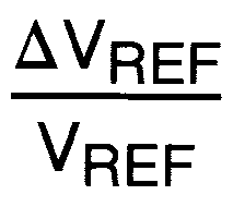 |
Reference voltage line regulation | VIN = 2.5 V to VOUT + 1 V | 0.03% | 0.1% | 0.03% | 0.2% | ||||
| VIN = VOUT(NOM)+ 1 V to 30 V(9) | 0.03% | 0.2% | 0.03% | 0.4% | ||||||
 |
Reference voltage load regulation | TJ = 25°C, IREF = 0 to 200 μA | 0.25% | 0.4% | 0.25% | 0.8% | ||||
| IREF = 0 to 200 μA | 0.25% | 0.6% | 0.25% | 1.0% | ||||||
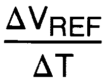 |
Reference voltage temperature coefficient | See(2), –40°C ≤ TJ ≤ 125°C | 20 | 20 | ppm/°C | |||||
| IB(FB) | Feedback pin bias current | TJ = 25°C | 20 | 40 | 20 | 40 | nA | |||
| 20 | 60 | 20 | 60 | |||||||
| IO(SINK) | Output off pulldown current | TJ = 25°C; see (10) | 30 | 30 | mA | |||||
| See (10) | 20 | 20 | ||||||||
| DROPOUT DETECTION COMPARATOR | ||||||||||
| IOH | Output high leakage | TJ = 25°C, VOH = 30 V | 0.01 | 1 | 0.01 | 1 | μA | |||
| VOH = 30 V | 0.01 | 2 | 0.01 | 2 | ||||||
| VOL | Output low voltage | TJ = 25°C, VIN = VOUT(NOM) − 0.5 V IOUT(COMP) = 400 μA |
150 | 250 | 150 | 250 | mV | |||
| VIN = VOUT(NOM) − 0.5 V IOUT(COMP) = 400 μA |
150 | 400 | 150 | 400 | ||||||
| VTHR(MAX) | Upper threshold voltage | TJ = 25°C, see(11) | −80 | −60 | −35 | −80 | −60 | −35 | mV | |
| See(11) | −95 | −60 | −25 | −95 | −60 | −25 | ||||
| VTHR(MIN) | Lower threshold voltage | TJ = 25°C, see(11) | −110 | −85 | −55 | −110 | −85 | −55 | mV | |
| See(11) | −160 | −85 | −40 | −160 | −85 | −40 | ||||
| HYST | Hysteresis | See(11) | 15 | 15 | mV | |||||
| SHUTDOWN INPUT(12) | ||||||||||
| VOS | Input offset voltage | TJ = 25°C (Referred to VREF) |
−7.5 | ±3 | 7.5 | −7.5 | ±3 | 7.5 | mV | |
| −10 | 10 | −10 | 10 | |||||||
| HYST | Hysteresis | 6 | 6 | mV | ||||||
| IB | Input bias current | TJ = 25°C VIN(SD) = 0 V to 5 V |
−30 | 10 | 30 | −30 | 10 | −30 | nA | |
| VIN(SD) = 0 V to 5 V | −50 | 50 | −50 | 50 | ||||||
| AUXILIARY COMPARATOR (LP2953 Only) | ||||||||||
| VOS | Input offset voltage | TJ = 25°C (Referred to VREF) |
−7.5 | ±3 | 7.5 | −7.5 | ±3 | 7.5 | mV | |
| (Referred to VREF) | −10 | ±3 | 10 | −10 | ±3 | 10 | ||||
| HYST | Hysteresis | 6 | 6 | mV | ||||||
| IB | Input bias current | TJ = 25°C, VIN(COMP) = 0 V to 5 V | −30 | 10 | 30 | −30 | 10 | 30 | nA | |
| VIN(COMP) = 0 V to 5 V | −50 | 10 | 50 | −50 | 10 | 50 | ||||
| IOH | Output high leakage | TJ = 25°C, VOH = 30 V | 0.01 | 1 | 0.01 | 1 | μA | |||
| VIN(COMP) = 1.3 V | 0.01 | 2 | 0.01 | 2 | ||||||
| VOL | Output low voltage | TJ = 25°C, VIN(COMP) = 1.1 V | 150 | 250 | 150 | 250 | mV | |||
| IOUT(COMP) = 400 μA | 150 | 400 | 150 | 400 | ||||||
(1) Drive SHUTDOWN pin with TTL or CMOS low level to shut off regulator, high level to turn on regulator.
(2) Output or reference voltage temperature coefficient is defined as the worst-case voltage change divided by the total temperature range.
(3) Load regulation is measured at constant junction temperature using low duty-cycle pulse testing. Two separate tests are performed, one for the range of IOUT = 100 μA to 1 mA and one for the range of IOUT =1 mA to 250 mA. Changes in output voltage due to heating effects are covered by the thermal regulation specification.
(4) Dropout voltage is defined as the input-to-output differential at which the output voltage drops 100 mV below the value measured with a 1-V differential. At very low values of programmed output voltage, the input voltage minimum of 2 V (2.3 V over temperature) must be observed.
(5) Ground pin current is the regulator quiescent current. The total current drawn from the source is the sum of the ground pin current, output load current, and current through the external resistive divider (if used).
(6) Thermal regulation is the change in output voltage at a time t after a change in power dissipation, excluding load or line regulation effects. Specifications are for a 200-mA load pulse at VIN = VOUT(NOM) + 15 V (3-W pulse) for t = 10 ms.
(7) Connect a 0.1-μF capacitor from the OUT pin to the FEEDBACK pin.
(8) VREF ≤ VOUT ≤ (VIN − 1 V), 2.3 V ≤ VIN ≤ 30 V, 100 μA ≤ IOUT ≤ 250 mA.
(9) Two separate tests are performed, one covering 2.5 V ≤ VIN ≤ VOUT(NOM)) + 1 V and the other test for VOUT(NOM) + 1 V ≤ VIN ≤ 30 V.
(10) VSHUTDOWN ≤ 1.1 V, VOUT = VOUT(NOM)
(11) Comparator thresholds are expressed in terms of a voltage differential at the FEEDBACK pin below the nominal reference voltage measured at VIN = VOUT(NOM) + 1 V. To express these thresholds in terms of output voltage change, multiply by the error amplifier gain, which is VOUT / VREF = (R1 + R2) / R2 (see Figure 31).
6.8 Typical Characteristics
Unless otherwise specified: VIN = 6 V, IOUT = 1 mA, COUT = 2.2 μF, VSD = 3 V, TA = 25°C, VOUT = 5 V.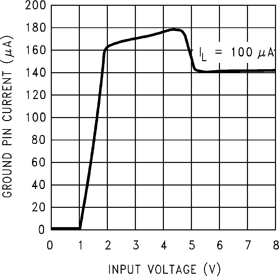 Figure 1. Quiescent Current
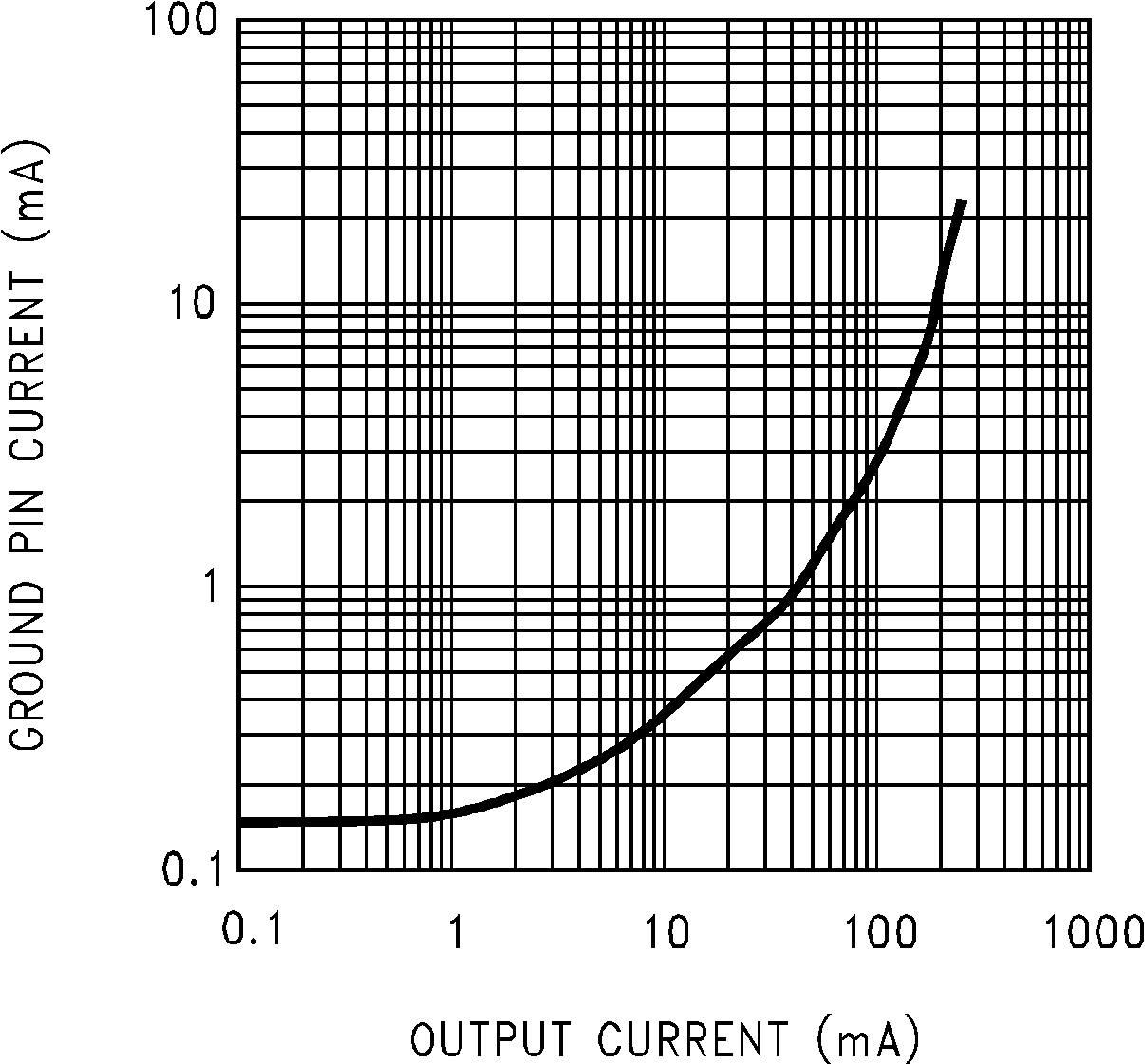 Figure 3. Ground Pin Current vs Load
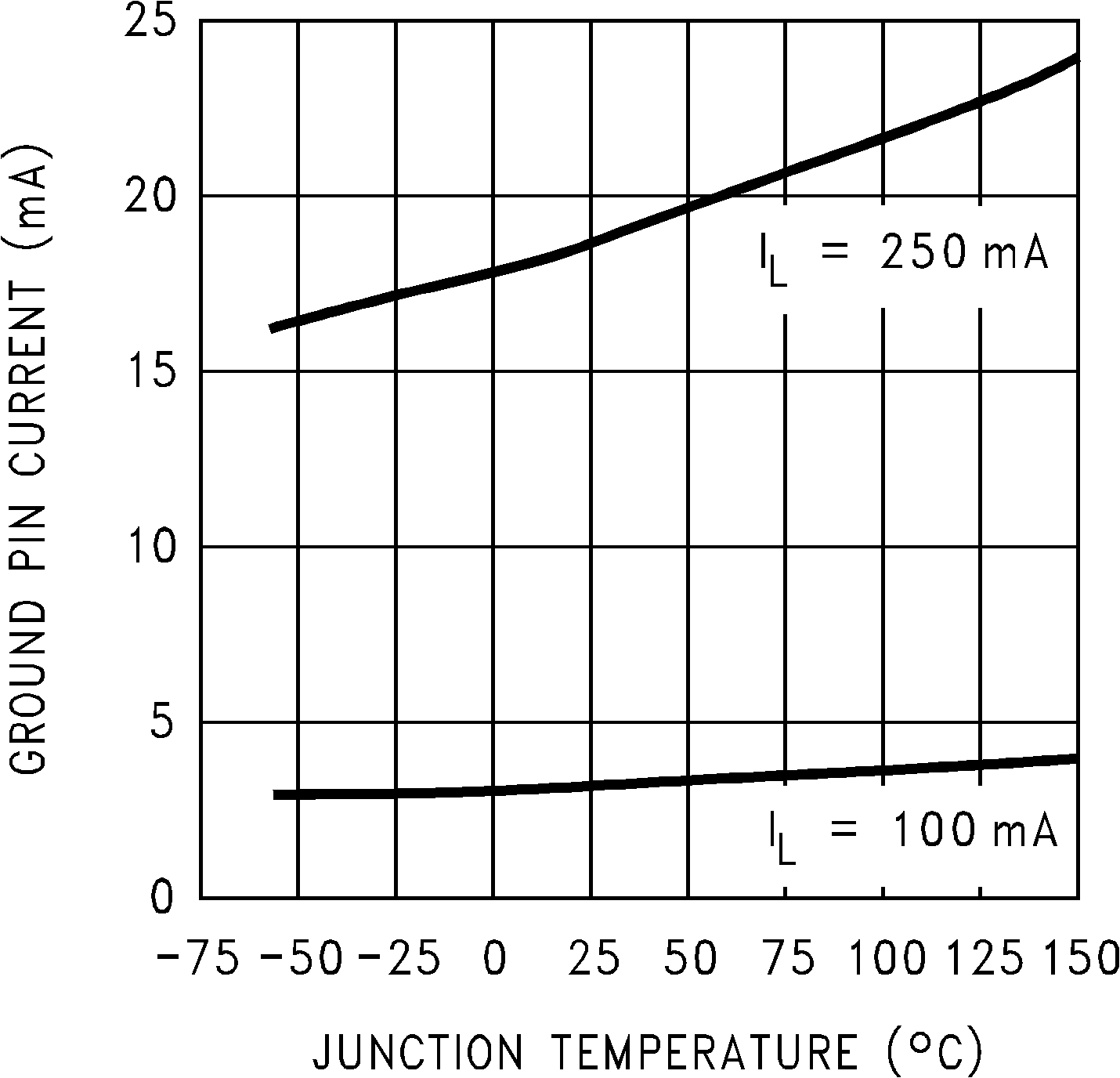 Figure 5. Ground Pin Current
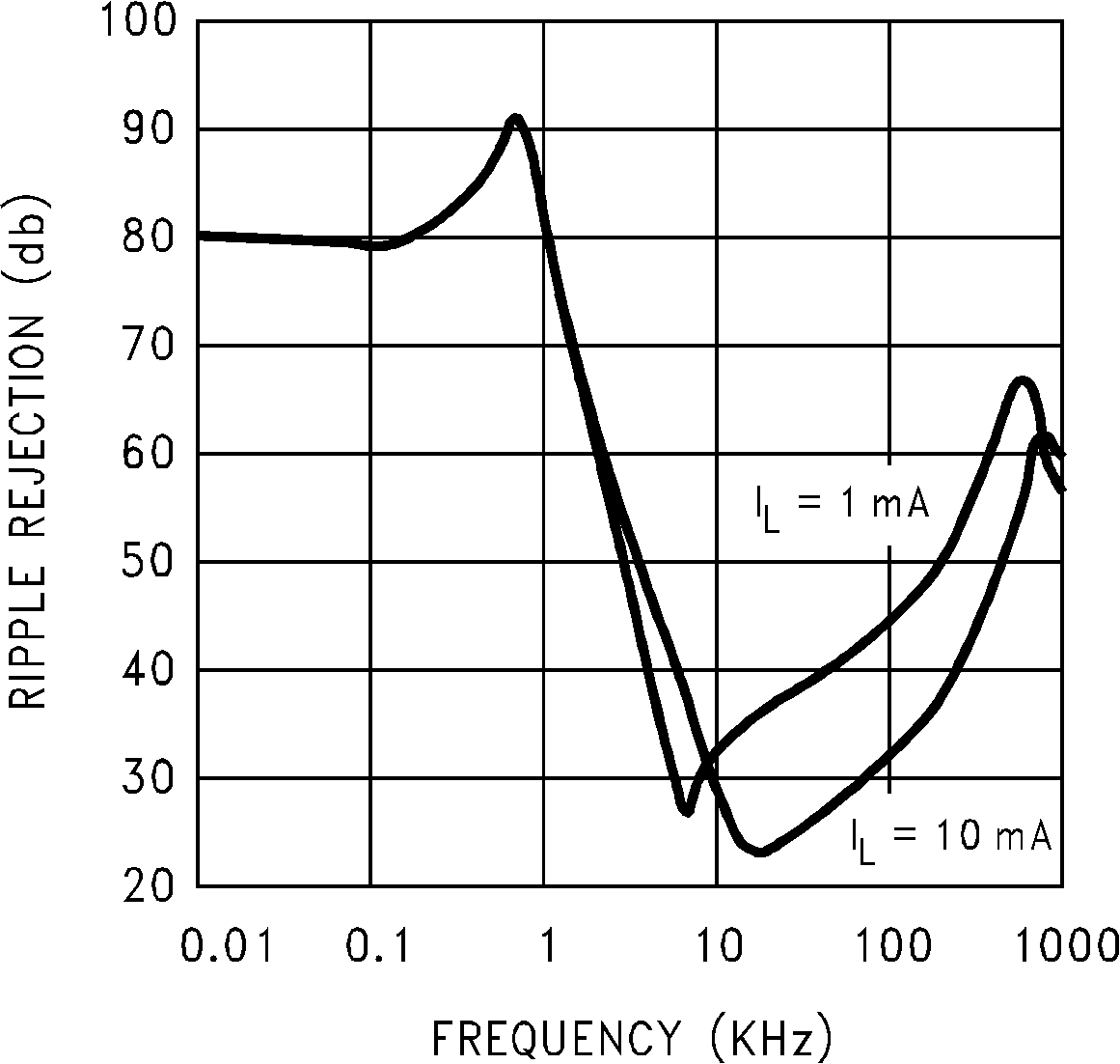 Figure 7. Ripple Rejection
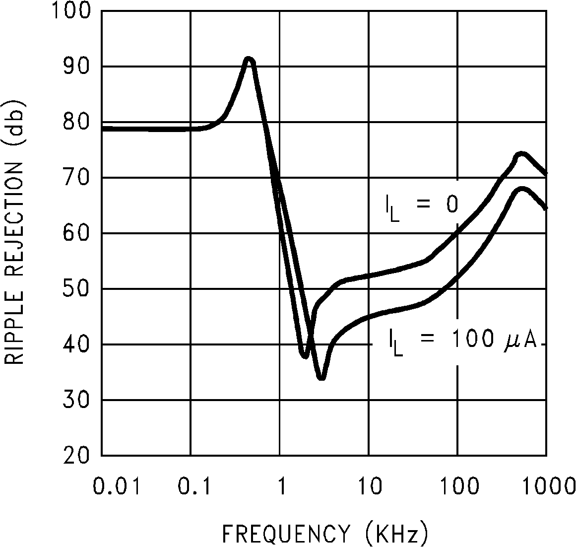 Figure 9. Ripple Rejection
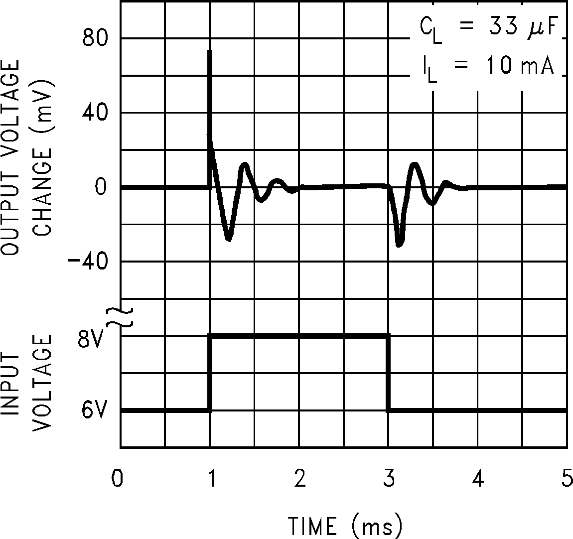 Figure 11. Line Transient Response
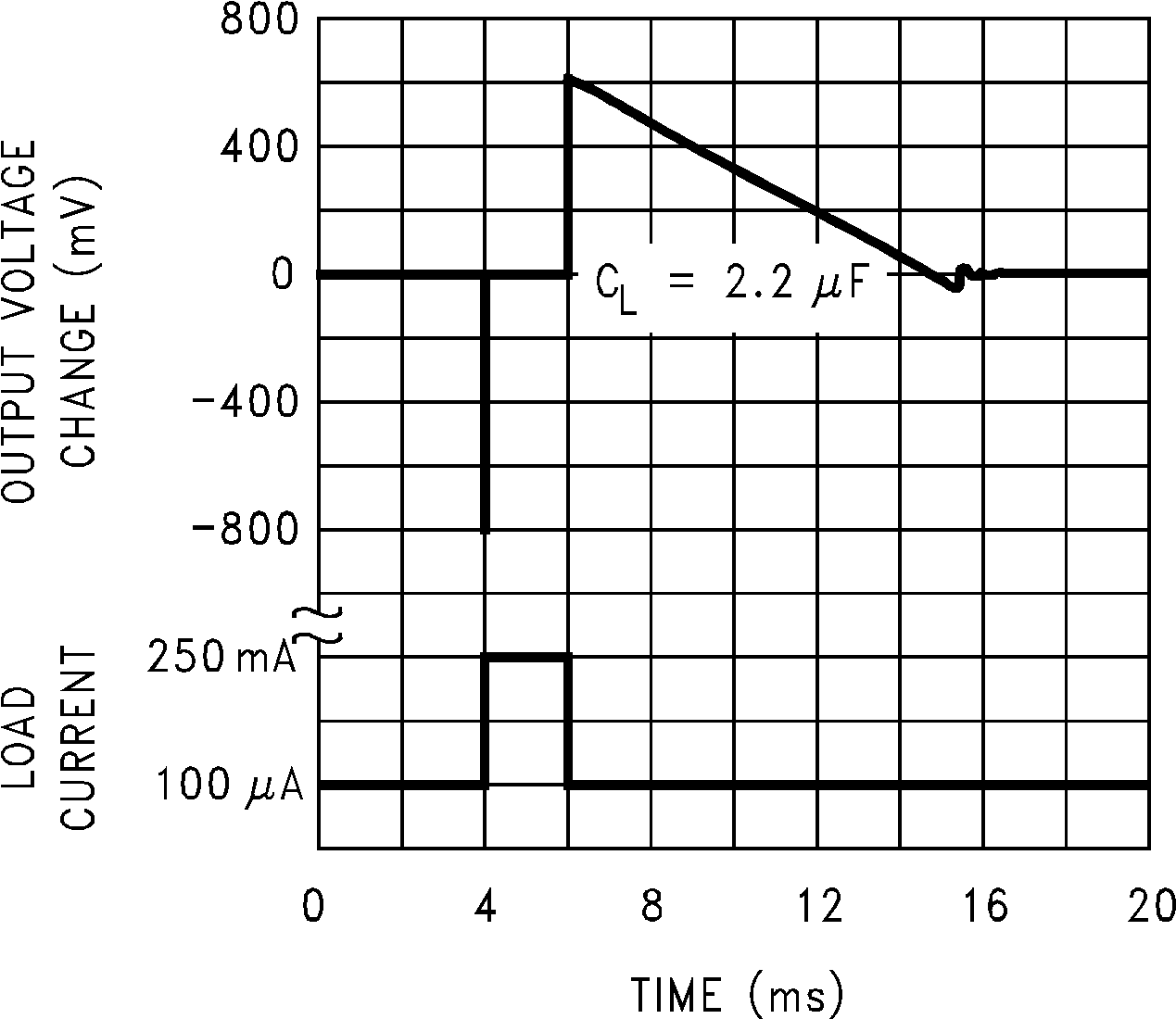 Figure 13. Load Transient Response
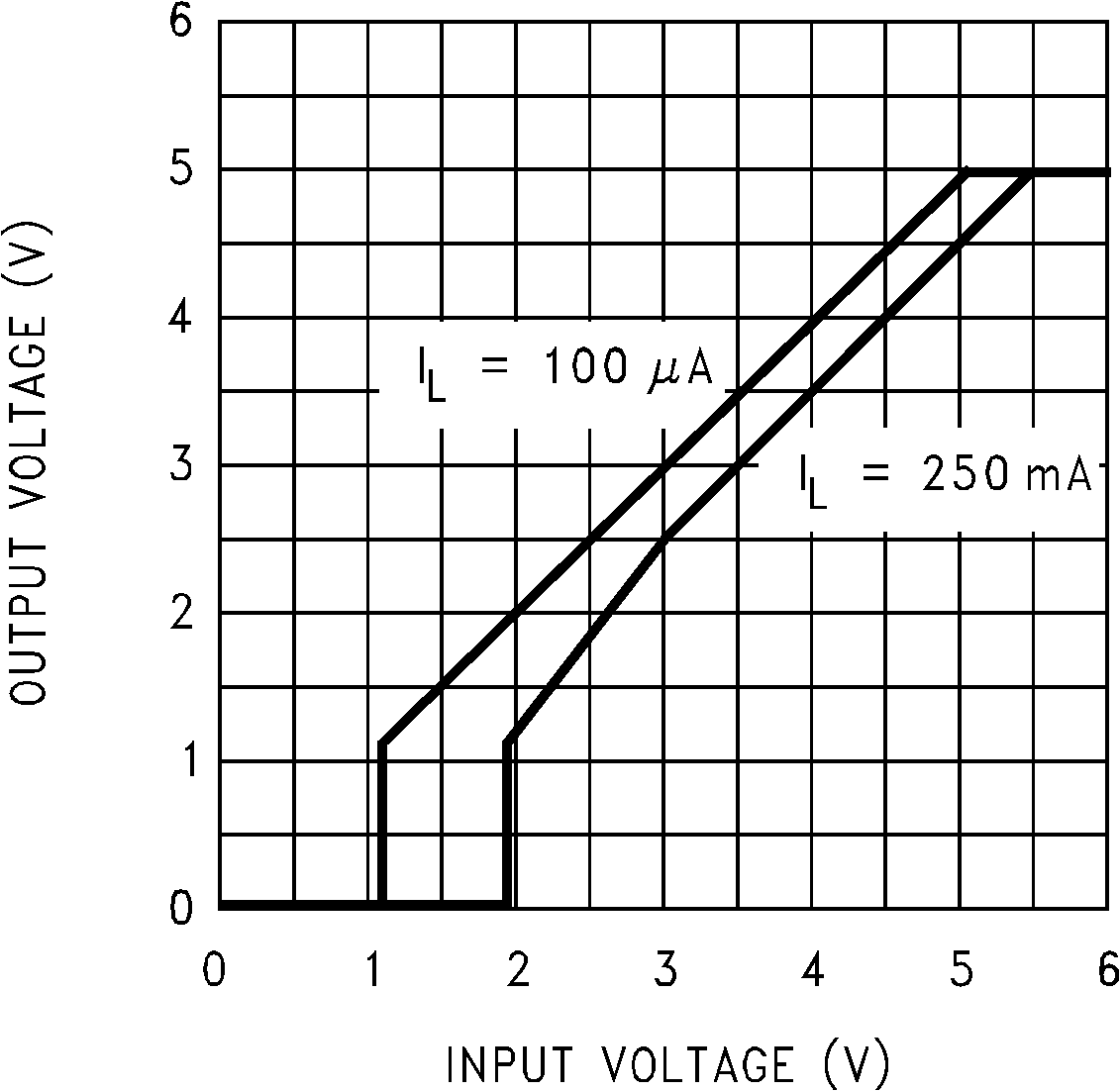 Figure 15. Dropout Characteristics
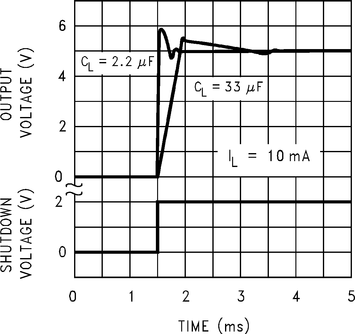 Figure 17. Enable Transient
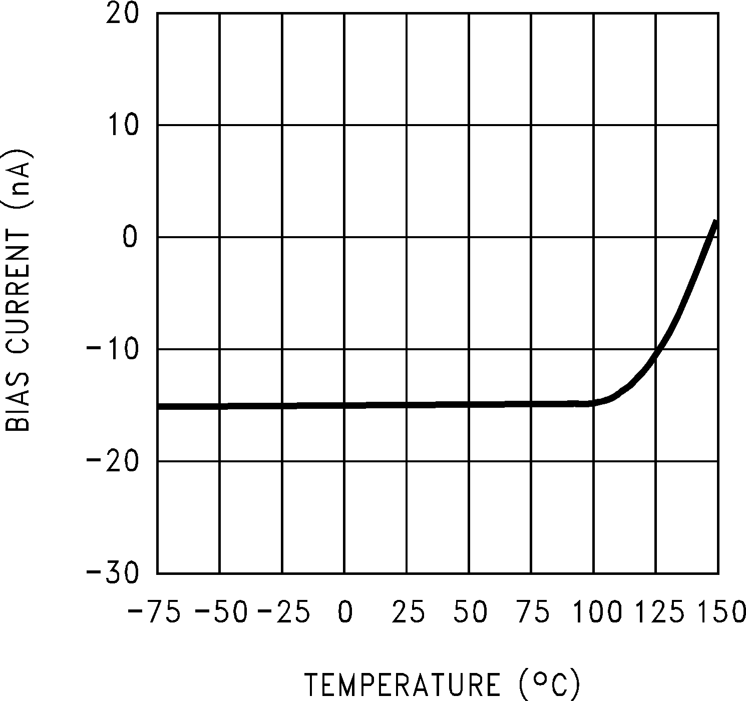 Figure 19. Feedback Bias Current
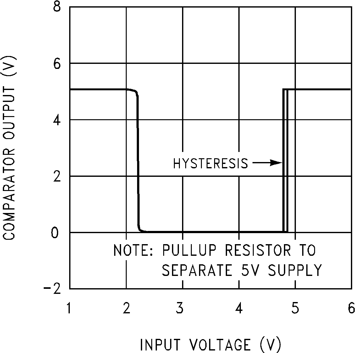 Figure 21. Error Output
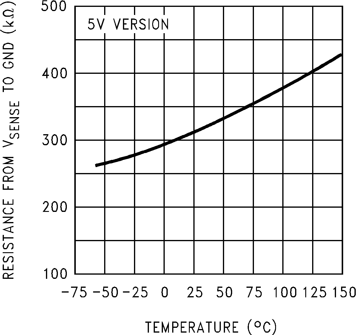 Figure 23. Divider Resistance
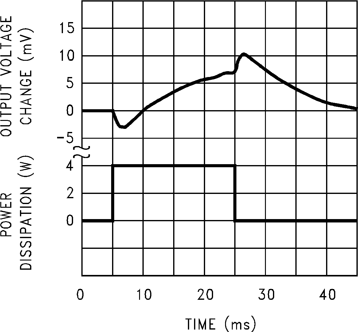 Figure 25. Thermal Regulation
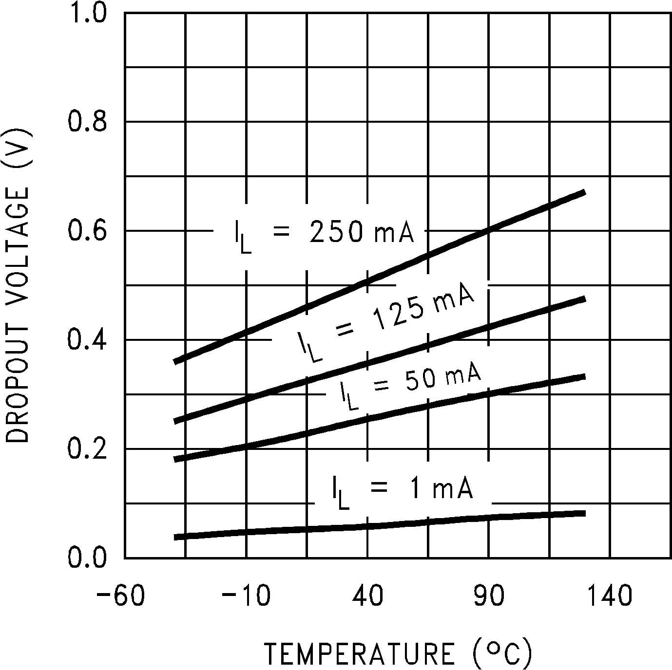 Figure 27. Dropout Voltage
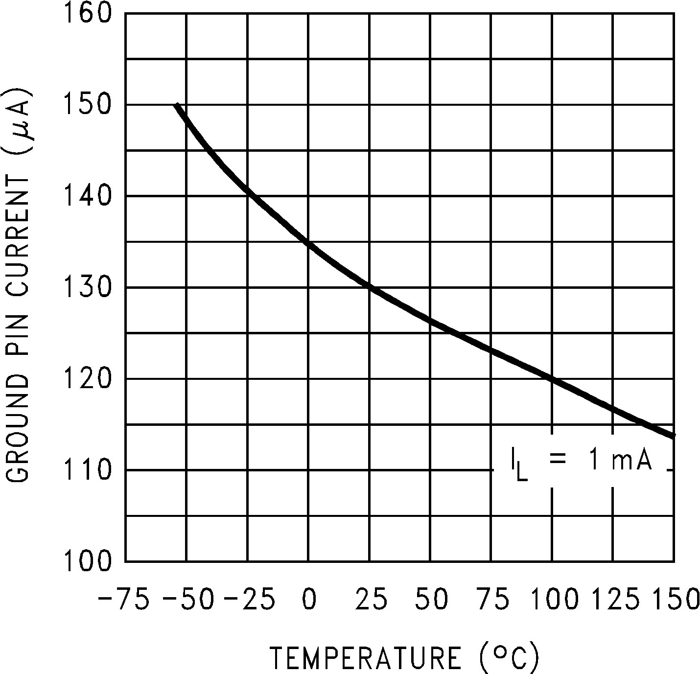 Figure 2. Quiescent Current
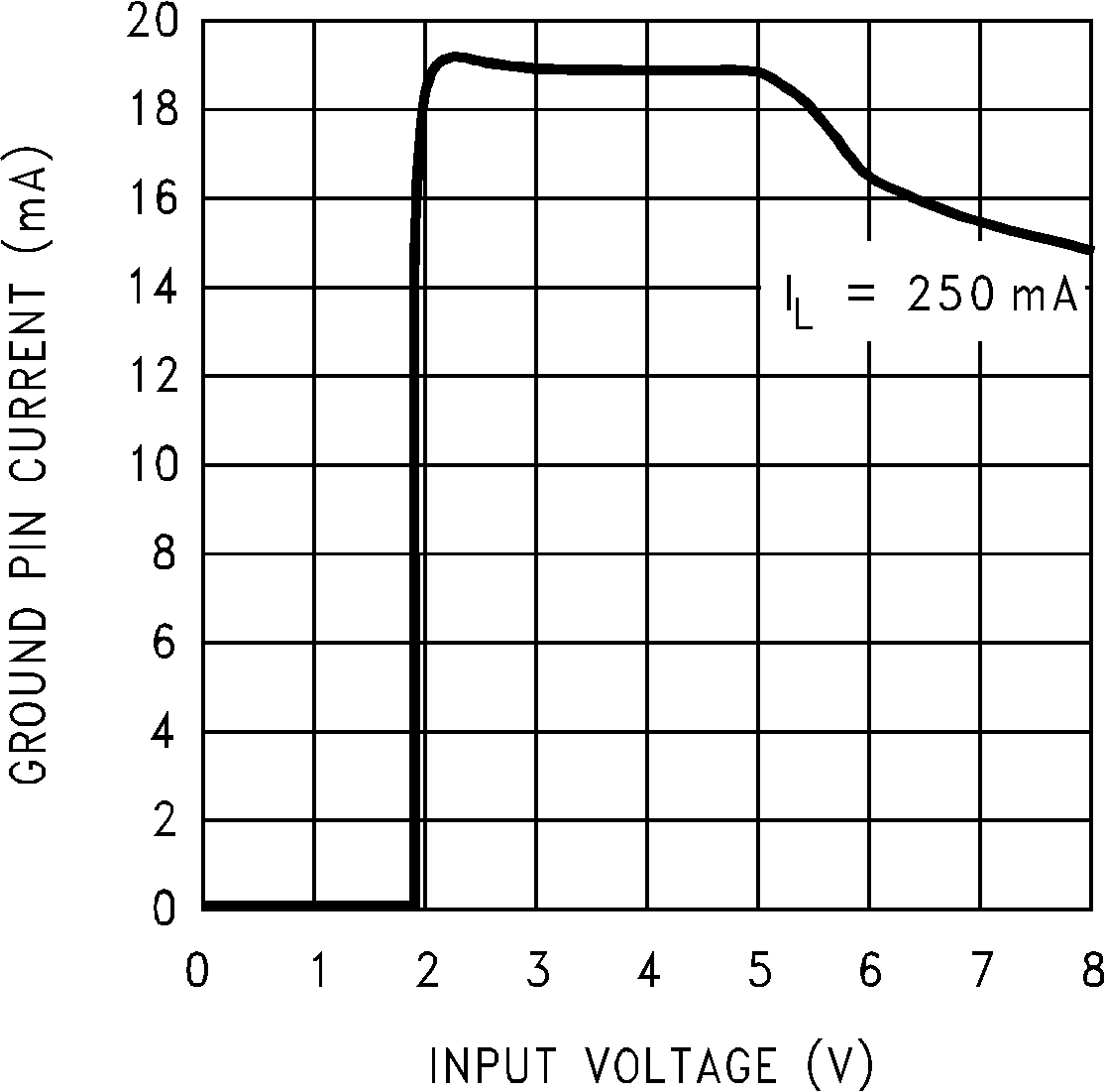 Figure 4. Ground Pin Current
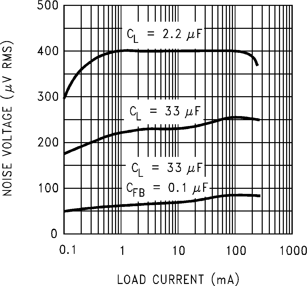 Figure 6. Output Noise Voltage
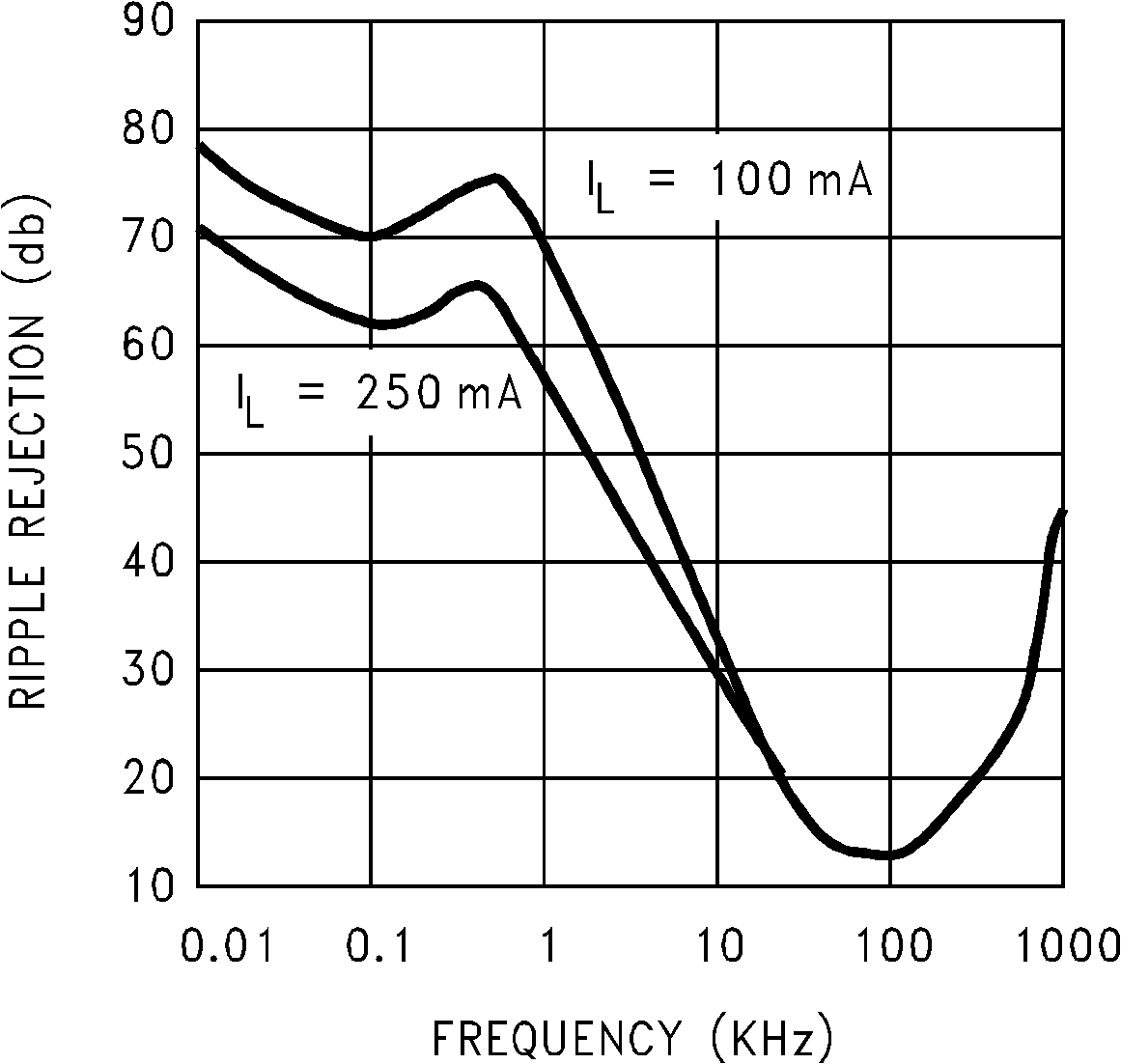 Figure 8. Ripple Rejection
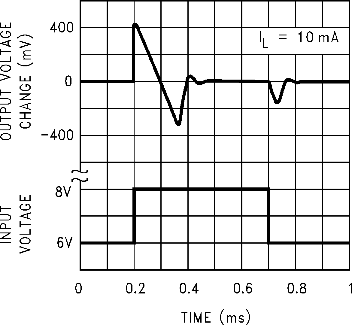 Figure 10. Line Transient Response
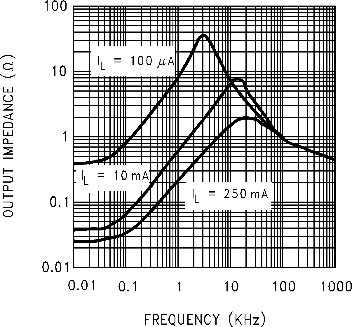 Figure 12. Output Impedance
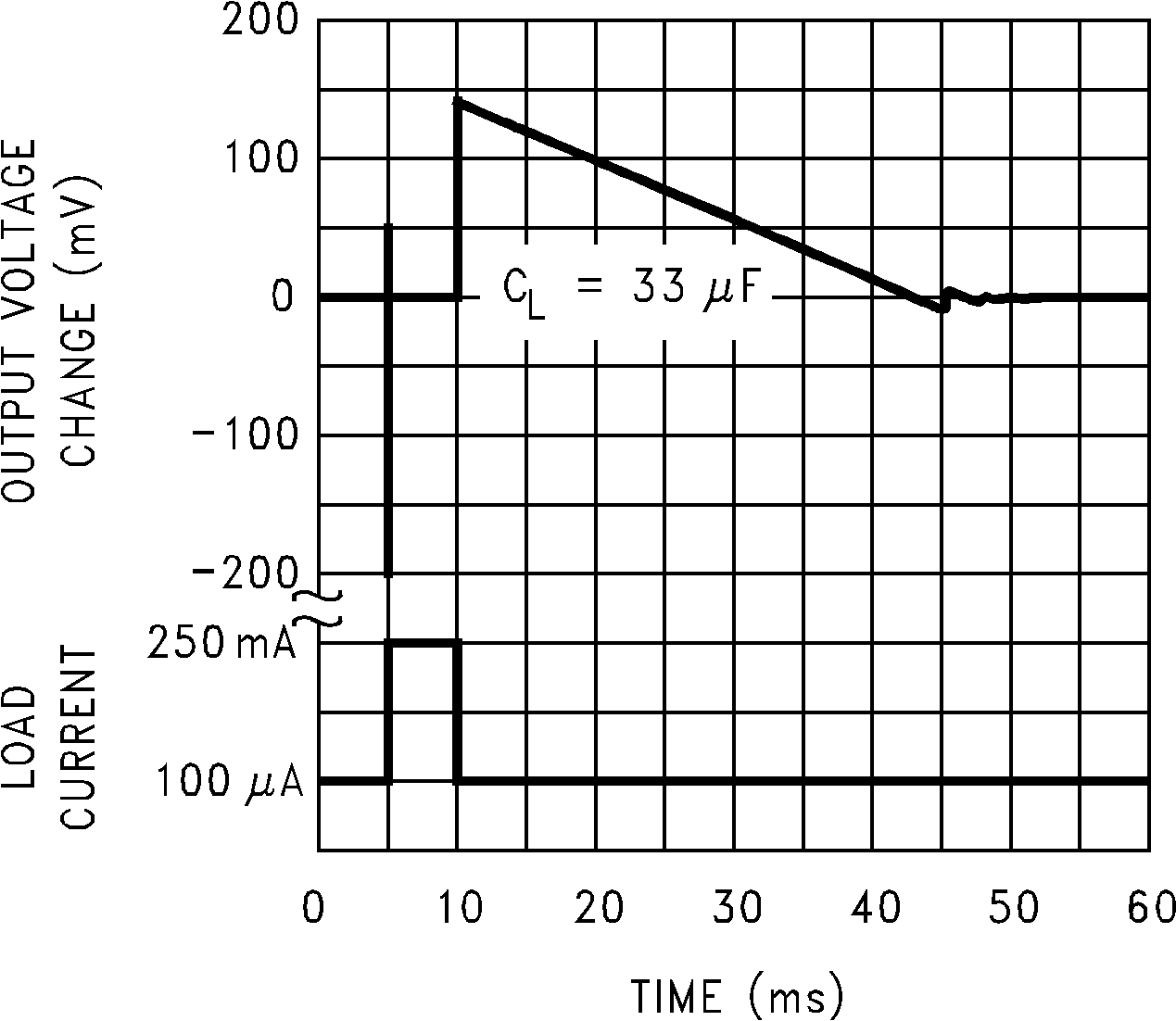 Figure 14. Load Transient Response
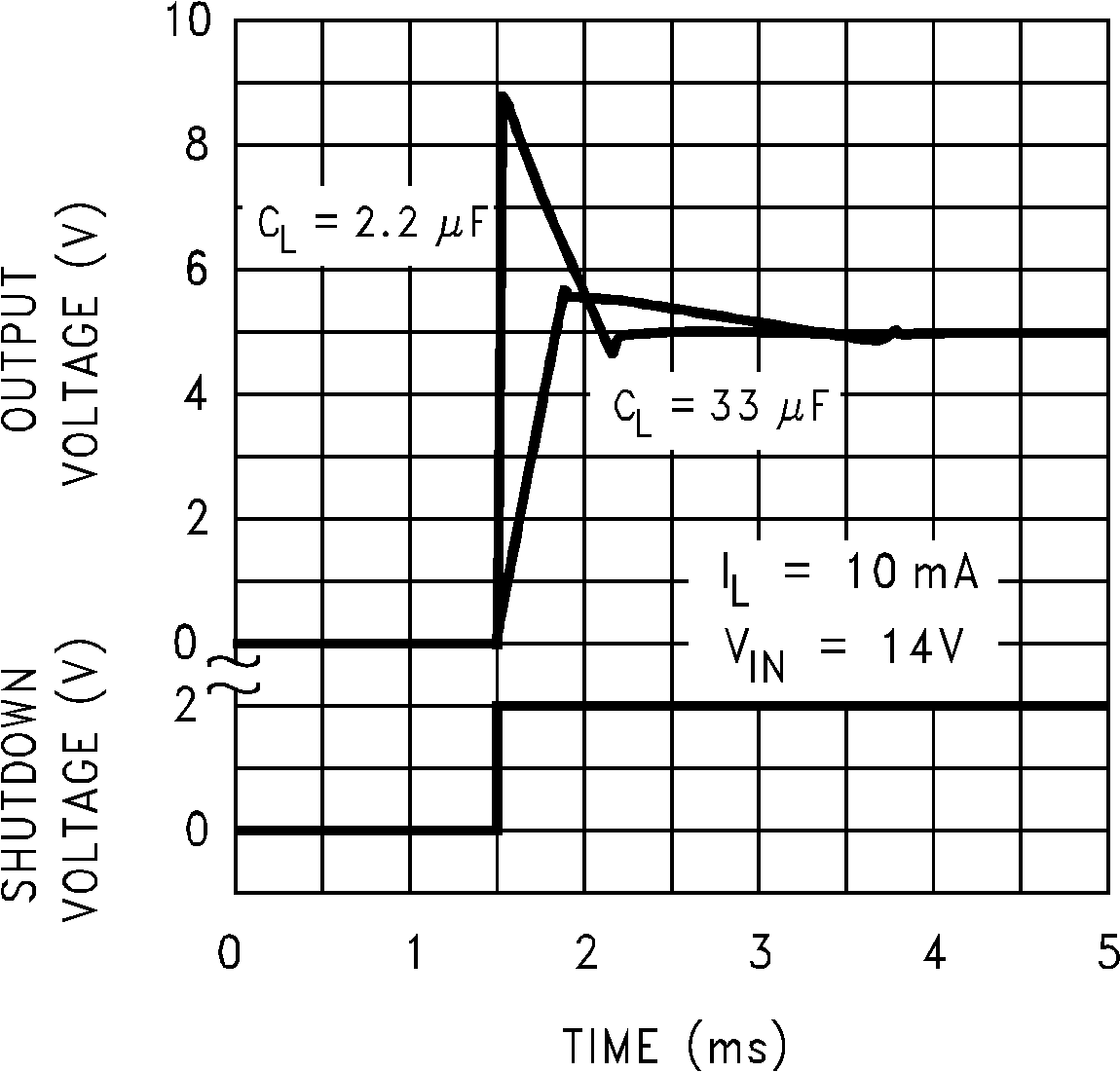 Figure 16. Enable Transient
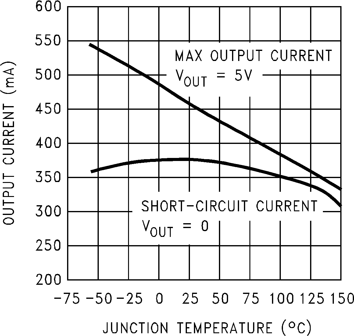 Figure 18. Short-Circuit Output Current and Maximum Output Current
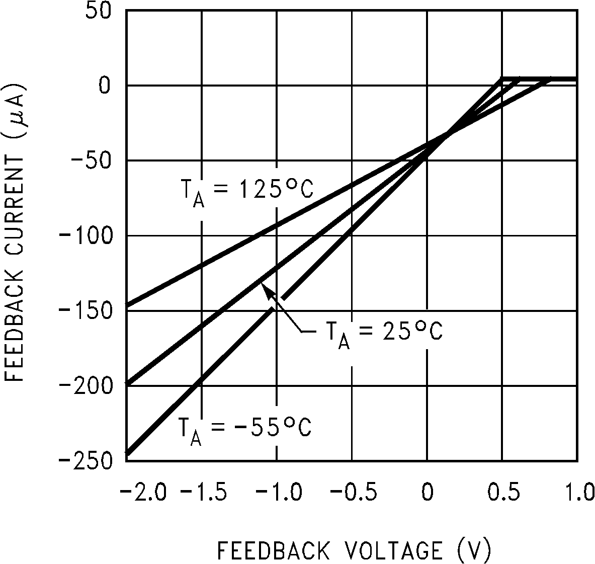 Figure 20. FEEDBACK Pin Current
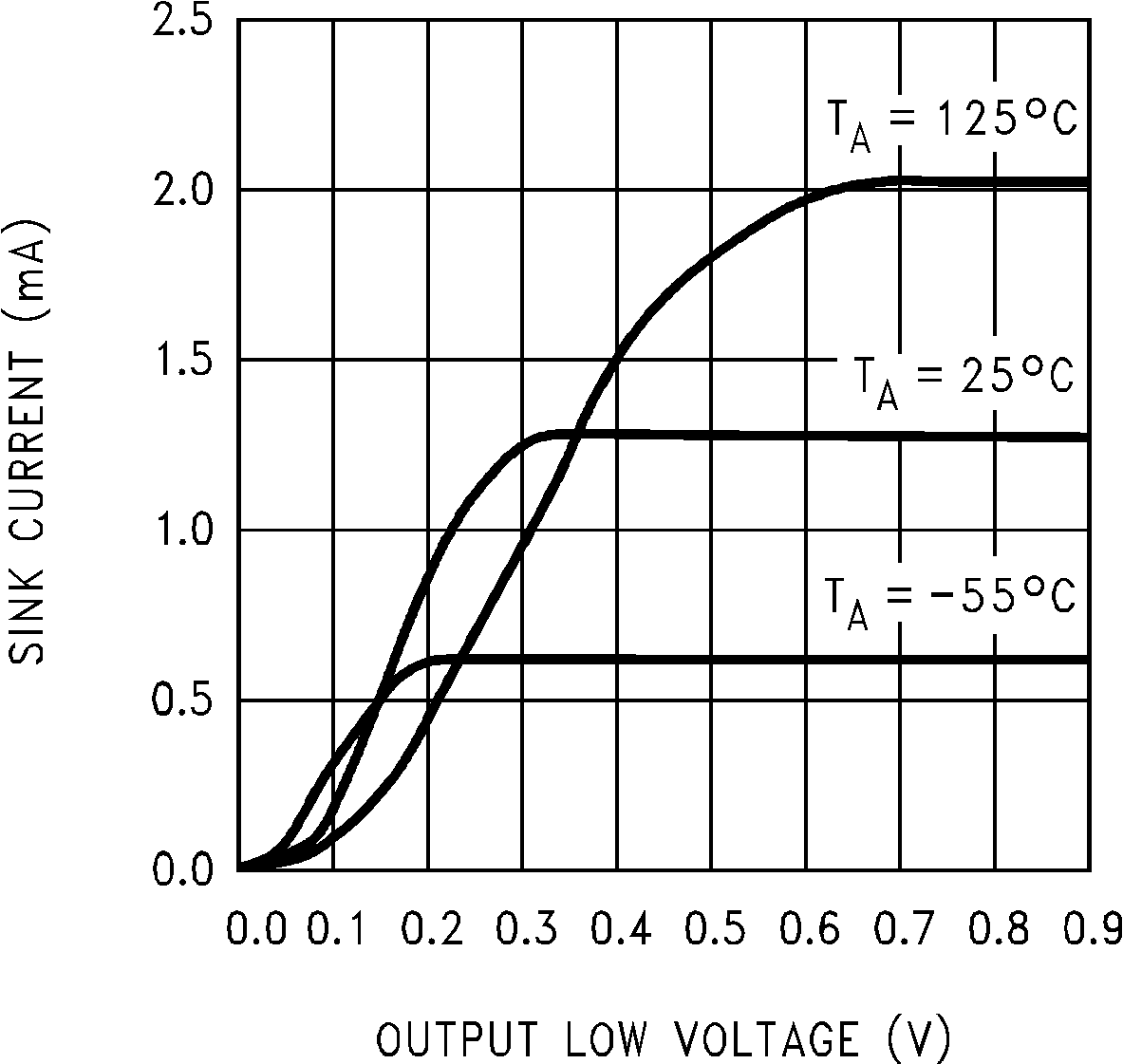 Figure 22. Comparator Sink Current
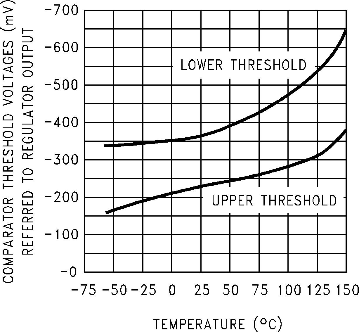 Figure 24. Dropout Detection Comparator Threshold Voltages
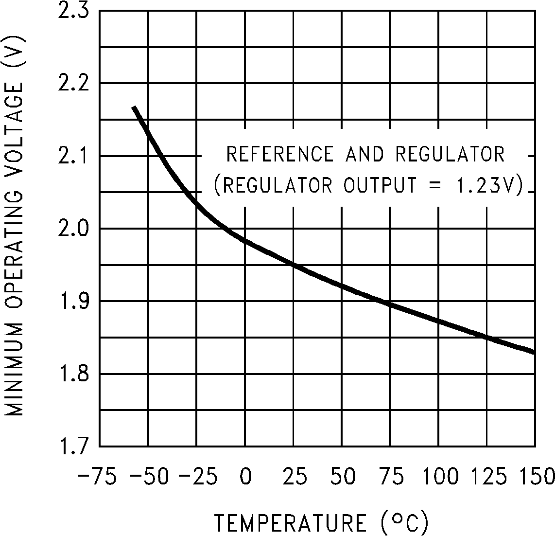 Figure 26. Minimum Operating Voltage