SNVS468L September 2006 – November 2015 LP3972
PRODUCTION DATA.
- 1 Features
- 2 Applications
- 3 Description
- 4 Revision History
- 5 Device Comparison Tables
- 6 Pin Configuration and Functions
-
7 Specifications
- 7.1 Absolute Maximum Ratings
- 7.2 ESD Ratings
- 7.3 Recommended Operating Conditions
- 7.4 Thermal Information
- 7.5 Electrical Characteristics
- 7.6 Electrical Characteristics: LDO RTC
- 7.7 Electrical Characteristics: LDOs 1 to 5
- 7.8 Electrical Characteristics: Buck Converters SW1, SW2, SW3
- 7.9 Electrical Characteristics: Backup Charger
- 7.10 Electrical Characteristics: I2C Compatible Serial Interface (SDA and SCL)
- 7.11 Logic Inputs and Outputs DC Operating Conditions
- 7.12 I2C Compatible Serial Interface Timing Requirements (SDA and SCL)
- 7.13 Power-On Timing Delays
- 7.14 Typical Characteristics
-
8 Detailed Description
- 8.1 Overview
- 8.2 Functional Block Diagram
- 8.3 Feature Description
- 8.4 Device Functional Modes
- 8.5
Programming
- 8.5.1
LP3972 Reset Sequence
- 8.5.1.1
LP3972 Controls
- 8.5.1.1.1 Digital Interface Control Signals
- 8.5.1.1.2 Power Domain Enables
- 8.5.1.1.3 Power Domains Sequencing (Delay)
- 8.5.1.1.4 Power Supply Enable
- 8.5.1.1.5 Wake-up Functionality (PWR_ON, NTEST_JIG, SPARE and EXT_WAKEUP)
- 8.5.1.1.6 Internal Thermal Shutdown Procedure
- 8.5.1.1.7 Battery Switch and Backup Battery Charger
- 8.5.1.1.8 General Purpose I/O Functionality (GPIO1 And GPIO2)
- 8.5.1.1.9 Regulated Voltages OK
- 8.5.1.1.10 Thermal Management
- 8.5.1.1.11 Thermal Warning
- 8.5.1.1.12 LP3972 Thermal Flags Functional Diagram, Data from Initial Silicon
- 8.5.1.2 Initial Cold Start Power-On Sequence
- 8.5.1.3 Hardware Reset Sequence
- 8.5.1.4 Reset Sequence
- 8.5.1.1
LP3972 Controls
- 8.5.2 I2C Compatible Interface
- 8.5.1
LP3972 Reset Sequence
- 8.6
Register Maps
- 8.6.1
Serial Interface Register Selection Codes
- 8.6.1.1 System Control Status Register
- 8.6.1.2 Output Voltage Enable Register 1
- 8.6.1.3 Output Voltage Status Register
- 8.6.1.4 Output Voltage Enable Register 2
- 8.6.1.5 Output Voltage Status Register 2
- 8.6.1.6 DVM Voltage Change Control Register 1
- 8.6.1.7 Buck1 (VCC_APPS) Voltage 1
- 8.6.1.8 Buck1 (VCC_APPS) Target Voltage 2 Register
- 8.6.1.9 Buck1 (VCC_APPS) Voltage Ramp Control Register
- 8.6.1.10 VCC_comm Target Voltage 1 Dummy Register (CDTV1)
- 8.6.1.11 VCC_COMM Target Voltage 2 Dummy Register (CDTV2)
- 8.6.1.12 LDO5 (VCC_SRAM) Target Voltage 1 Register
- 8.6.1.13 LDO5 (VCC_SRAM) Target Voltage 2 Register
- 8.6.1.14 LDO1 (VCC_MVT) Target Voltage 1 Register (MDTV1)
- 8.6.1.15 LDO1 (VCC_MVT) Target Voltage 2 Register
- 8.6.1.16 LDO2 Voltage Control Register (L12VCR)
- 8.6.1.17 LDO4 - LDO3 Voltage Control Register (L34VCR)
- 8.6.2
TI-Defined Control and Status Registers
- 8.6.2.1 System Control Register 1 (SCR1)
- 8.6.2.2 System Control Register 2 (SCR2)
- 8.6.2.3 Output Enable 3 Register (OEN3) 8h’82
- 8.6.2.4 Output Enable 3 Register (OEN3) 8h’82 Definitions
- 8.6.2.5 Status Register 3 (OSR3) 8h’83
- 8.6.2.6 Status Register 3 (OSR3) Definitions 8h’83
- 8.6.2.7 Logic Output Enable Register (LOER) 8h’84
- 8.6.2.8 Logic Output Enable Register (LOER) Definitions 8h’84
- 8.6.2.9 VCC_BUCK2 Target Voltage Register (B2TV) 8h’85
- 8.6.2.10 VCC_BUCK2 Target Voltage Register (B2TV) 8h’85 Definitions
- 8.6.2.11 BUCK3 Target Voltage Register (B3TV) 8h’86
- 8.6.2.12 BUCK3 Target Voltage Register (B3TV) 8h’86 Definitions
- 8.6.2.13 VCC_BUCK3:2 Voltage Ramp Control Register (B32RC)
- 8.6.2.14 Interrupt Status Register ISRA
- 8.6.2.15 Backup Battery Charger Control Register (BCCR)
- 8.6.2.16 Marvell PXA Internal 1 Revision Register (II1RR) 8h’8E
- 8.6.2.17 Marvell PXA Internal 1 Revision Register (II1RR) (Ii1rr) 8h’8E Definitions
- 8.6.2.18 Marvell PXA Internal 2 Revision Register (II1RR) 8h’8F
- 8.6.2.19 Marvell PXA Internal 2 Revision Register (II1RR) 8h’8F Definitions
- 8.6.2.20 Register Programming Examples
- 8.6.1
Serial Interface Register Selection Codes
- 9 Application and Implementation
- 10Power Supply Recommendations
- 11Layout
- 12Device and Documentation Support
- 13Mechanical, Packaging, and Orderable Information
8 Detailed Description
8.1 Overview
The LP3972 includes three high-efficiency step-down DC-DC switching buck converters. Using a voltage mode architecture with synchronous rectification, the buck converters have the ability to deliver up to 1600 mA depending on the input voltage, output voltage, ambient temperature, and the inductor chosen.
There are three modes of operation depending on the current required: PWM, PFM, and shutdown. The device operates in PWM mode at load currents of approximately 100 mA or higher, having voltage tolerance of ±3% with 95% efficiency or better. Lighter load currents cause the device to automatically switch into PFM for reduced current consumption. Shutdown mode turns off the device, offering the lowest current consumption (IQ, SHUTDOWN = 0.01 µA typical).
Additional features include soft-start, undervoltage protection, current-overload protection, and thermal-shutdown protection.
The part uses an internal reference voltage of 0.5 V. TI recommends that the device be kept in shutdown until the input voltage is 2.7 V or higher.
8.2 Functional Block Diagram
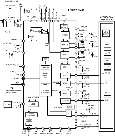
- The I2C lines are pulled up via a I/O source.
- VINLDOs 4, 5 can either be powered from main battery source or by a buck regulator or VIN.
8.3 Feature Description
8.3.1 Buck Converter Operation
8.3.1.1 Circuit Operation
The buck converter operates as follows: during the first portion of each switching cycle, the control block turns on the internal PFET switch. This allows current to flow from the input through the inductor to the output filter capacitor and load. The inductor limits the current to a ramp with a slope of (VIN – VOUT)/L, by storing energy in a magnetic field.
During the second portion of each cycle, the controller turns the PFET switch off, blocking current flow from the input, and then turns the NFET synchronous rectifier on. The inductor draws current from ground through the NFET to the output filter capacitor and load, which ramps the inductor current down with a slope of –VOUT/L.
The output filter stores charge when the inductor current is high, and releases it when inductor current is low, smoothing the voltage across the load.
The output voltage is regulated by modulating the PFET switch on time to control the average current sent to the load. The effect is identical to sending a duty-cycle modulated rectangular wave formed by the switch and synchronous rectifier at the SW pin to a low-pass filter formed by the inductor and output filter capacitor. The output voltage is equal to the average voltage at the SW pin.
8.3.1.2 PWM Operation
During pulse width modulation (PWM) operation the converter operates as a voltage mode controller with input voltage feed forward. This allows the converter to achieve good load and line regulation. The DC gain of the power stage is proportional to the input voltage. To eliminate this dependence, feed forward inversely proportional to the input voltage is introduced.
While in PWM mode, the output voltage is regulated by switching at a constant frequency and then modulating the energy per cycle to control power to the load. At the beginning of each clock cycle the PFET switch is turned on, and the inductor current ramps up until the comparator trips and the control logic turns off the switch. The current limit comparator can also turn off the switch in case the current limit of the PFET is exceeded. Then the NFET switch is turned on and the inductor current ramps down. The next cycle is initiated by the clock turning off the NFET and turning on the PFET.
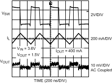 Figure 11. Typical PWM Operation
8.3.1.2.1 Internal Synchronous Rectification
While in PWM mode, the converters uses an internal NFET as a synchronous rectifier to reduce rectifier forward voltage drop and associated power loss. Synchronous rectification provides a significant improvement in efficiency whenever the output voltage is relatively low compared to the voltage drop across an ordinary rectifier diode.
8.3.1.2.2 Current Limiting
A current limit feature allows the converters to protect itself and external components during overload conditions. PWM mode implements current limiting using an internal comparator that trips at 2 A (typical). If the output is shorted to ground the device enters a timed current limit mode where the NFET is turned on for a longer duration until the inductor current falls below a low threshold, ensuring inductor current has more time to decay, thereby preventing runaway.
8.3.1.3 PFM Operation
At very light loads, the converter enters pulse frequency modulation (PFM) mode and operates with reduced switching frequency and supply current to maintain high efficiency.
The part automatically transitions into PFM mode when either of two conditions occurs for a duration of 32 or more clock cycles:
- The inductor current becomes discontinuous.
- The peak PMOS switch current drops below the IMODE level (typically IMODE < 30 mA + VIN/42 Ω).
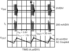 Figure 12. Typical PFM Operation
During PFM operation, the converter positions the output voltage slightly higher than the nominal output voltage during PWM operation, allowing additional headroom for voltage drop during a load transient from light to heavy load. The PFM comparators sense the output voltage via the feedback pin and control the switching of the output FETs such that the output voltage ramps between < 0.6% and <1.7% above the nominal PWM output voltage. If the output voltage is below the high PFM comparator threshold, the PMOS power switch is turned on. It remains on until the output voltage reaches the high PFM threshold or the peak current exceeds the IPFM level set for PFM mode. The typical peak current in PFM mode is: IPFM = 112 mA + VIN/27 Ω. Once the PMOS power switch is turned off, the NMOS power switch is turned on until the inductor current ramps to zero. When the NMOS zero-current condition is detected, the NMOS power switch is turned off. If the output voltage is below the high PFM comparator threshold (see Figure 13), the PMOS switch is again turned on and the cycle is repeated until the output reaches the desired level. Once the output reaches the ‘high’ PFM threshold, the NMOS switch is turned on briefly to ramp the inductor current to zero and then both output switches are turned off and the part enters an extremely low power mode. Quiescent supply current during this sleep mode is 21 µA (typical), which allows the part to achieve high efficiencies under extremely light load conditions. When the output drops below the low PFM threshold, the cycle repeats to restore the output voltage (average voltage in PFM mode) to < 1.15% above the nominal PWM output voltage. If the load current increases during PFM mode (see Figure 13) causing the output voltage to fall below the low2 PFM threshold, the device automatically transitions into fixed-frequency PWM mode. Typically when VIN = 3.6 V the device transitions from PWM-to-PFM mode at 100-mA output current.
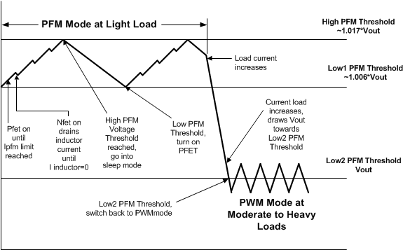 Figure 13. Operation in PFM Mode and Transfer to PWM Mode
8.3.1.4 Soft Start
The buck converter has a soft-start circuit that limits in-rush current during start-up. During start-up the switch current limit is increased in steps. Soft start is activated only if EN goes from logic low to logic high after VIN reaches 2.7 V. Soft start is implemented by increasing switch current limit in steps of 213 mA, 425 mA, 850 mA and 1700 mA (typical switch current limit). The start-up time thereby depends on the output capacitor and load current demanded at start-up. Typical start-up time with a 10-µF output capacitor and 1000-mA load current is 390 µs and with a 1-mA load current, it is 295 µs.
8.3.1.5 Low Dropout (LDO) Operation
The LP3972 can operate at 100% duty cycle (no switching; PMOS switch completely on) for LDO support of the output voltage. In this way the output voltage is controlled down to the lowest possible input voltage. When the device operates near 100% duty cycle, output voltage ripple is approximately 25 mV. The minimum input voltage needed to support the output voltage is
where
- ILOAD = Load Current
- RDSON, PFET = drain-to-source resistance of PFET switch in the triode region
- RINDUCTOR = Inductor resistance
8.3.1.6 Spread-Spectrum Feature
Periodic switching in the buck regulator is inherently a noisier function block compared to an LDO. It can be challenging in some critical applications to comply with stringent regulatory standards or simply to minimize interference to sensitive circuits in space limited portable systems. The regulator’s switching frequency and harmonics can cause noise in the signal spectrum. The magnitude of this noise is measured by its power spectral density. The power spectral density of the switching frequency, FC, is one parameter that system designers want to be as low as practical to reduce interference to the environment and subsystems within their products. The LP3972 has a user selectable function on chip, wherein a noise reduction technique known as spread spectrum can be employed to ease customer’s design and production issues.
The principle behind spread spectrum is to modulate the switching frequency slightly and slowly, and spread the signal frequency over a broader bandwidth. Thus, its power spectral density becomes attenuated, and the associated interference electro-magnetic energy is reduced. The clock used to modulate the LP3972 buck regulator can be used as a spread spectrum clock via 2 I2C control register (System Control Register 1 (SCR1) 8h’80) bits bk_ssen, and slomod. With this feature enabled, the intense energy of the clock frequency can be spread across a small band of frequencies in the neighborhood of the center frequency. This results in a reduction of the peak energy.
The LP3972 spread-spectrum clock uses a triangular modulation profile with equal rise and fall slopes. The modulation has the following characteristics:
- The center frequency: fC = 2 MHz, and
- The modulating frequency, ƒM = 6.8 kHz or 12 kHz.
- Peak frequency deviation: Δ_ƒ = ±100 kHz (or ±5%)
- Modulation index β = Δ_f/fM = 14.7 or 8.3
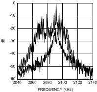 Figure 14. Switching Energy RBW = 300 Hz
8.3.2 LP3972 Battery Switch Operation
The LP3972 has provisions for two battery connections, the main battery VBAT and the backup battery.
The function of the battery switch is to connect power to the LDO_RTC from the appropriate battery, depending on conditions described as follows:
- If only the backup battery is applied, the switch automatically connect sthe LDO_RTC power to this battery.
- If only the main battery is applied, the switch automatically connects the LDO_RTC power to this battery
- If both batteries are applied, and the main battery is sufficiently charged (VBAT > 3.1 V), the switch automatically connects the LDO_RTC power to the main battery.
- As the main battery is discharged a separate circuit called nBATT_FLT warns the system. Then if no action is taken to restore the charge on the main battery, and discharging is continued the battery switch disconnects the input of the LDO_RTC from the main battery and connect to the backup battery.
- The main battery voltage at which the LDO_RTC is switched over from main to backup battery is 2.8 V typically.
- There is a hysteric voltage in this switch operation, thus the LDO_RTC is not reconnected to main battery until main battery voltage is greater than 3.1 V typically.
- The system designer may wish to disable the battery switch when only a main battery is used. This is accomplished by setting the no backup battery bit in the control register 8h’0B bit 7 NBUB. With this bit set to 1, the switching does not occur; that is, the LDO_RTC remains connected to the main battery even as it is discharged below the 2.9-V threshold. The backup battery input must also be connected to main battery.
8.4 Device Functional Modes
8.4.1 Start-Up Mode
Start-up mode is entered once the battery backup supply is connected to LP3972. The RTC LDO is then turned on to power the VCC_BATT pin of the application processor. Start-up state exits once nRSTO de-asserts (after a minimum of 50 ms) and when nBATT_FLT de-asserts once system power is available.
8.4.2 Shutdown Mode
During shutdown the PFET switch, reference, control and bias circuitry of the converters are turned off. The NFET switch opens in shutdown to discharge the output. When the converter is enabled, EN, soft start is activated. It is recommended to disable the converter during the system power up and undervoltage conditions when the supply is less than 2.7V.
8.4.3 Standby Mode
Once NRSTO and nBATT_FLT are de-asserted the LP3972 waits for SYS_EN signal in standby mode. All high-voltage power domains are still disabled in this state.
8.4.4 Active Mode
Once SYS_EN goes high the device begins turning on the high-voltage power supplies. Once PWR_EN goes high the LP3972 enables the low-voltage power supplies. The Apps processor must monitor the “Power OK” status bits before beginning execution of code to make sure all supplies have been properly enabled.
8.5 Programming
8.5.1 LP3972 Reset Sequence
8.5.1.1 LP3972 Controls
8.5.1.1.1 Digital Interface Control Signals
| SIGNAL | DEFINITION | ACTIVE STATE | SIGNAL DIRECTION |
|---|---|---|---|
| SYS_EN | High Voltage Power Enable | High | Input |
| PWR_EN | Low Voltage Power Enable | High | Input |
| SCL | Serial Bus Clock Line | Clock | Input |
| SDA | Serial Bus Data Line | Bidirectional | |
| nRSTI | Forces an unconditional hardware reset | Low | Input |
| nRSTO | Forces an unconditional hardware reset | Low | Output |
| nBATT_FLT | Main Battery removed or discharged indicator | Low | Output |
| PWR_ON | Wake-up Input to CPU | High | Input |
| nTEST_JIG | Wake-up Input to CPU | Low | Input |
| SPARE | Wake-up Input to CPU | High/Low | Input |
| EXT_WAKEUP | Wake-up Output for application processor | High | Output |
| GPIO1 / nCHG_EN | General Purpose I/O /External backup Battery Charger enable | — | Bidirectional /Input |
| GPIO2 | General Purpose I/O | — | Bidirectional |
8.5.1.1.2 Power Domain Enables
Table 3. Hardware and Software Enable Options for Each Supply
| PMU OUTPUT | HW ENABLE | SW ENABLE |
|---|---|---|
| LDO_RTC | — | — |
| LDO1 (VCC_MVT) | SYS_EN | LDO1_EN |
| LDO2 | SYS_EN | LDO2_EN |
| LDO3 | SYS_EN | LDO3_EN |
| LDO4 | SYS_EN | LDO4_EN |
| LDO5 (VCC_SRAM) | PWR_EN | S_EN |
| Buck1 (VCC_APPS) | PWR_EN | A_EN |
| BUCK2 | SYS_EN | B2_EN |
| BUCK3 | SYS_EN | B3_EN |
8.5.1.1.3 Power Domains Sequencing (Delay)
By default SYS_EN must be on to have PWR_EN enable but this feature can be switched off by register bit BP_SYS.
By default always enables SYS_EN LDO1 and, after a typical 1-ms delay, others. Also when SYS_EN is set off the LDO1 goes off last. This function can be switched off or delay can be changed by DELAY bits via serial interface as seen in Table 4.
8h’80 Bit 5:4
Table 4. Programmable Supply Delay Options
| DELAY (bits) | DELAY (ms) |
|---|---|
| 00 | 0 |
| 01 | 0.5 |
| 10 | 1 |
| 11 | 1.5 |
8.5.1.1.4 Power Supply Enable
SYS_EN and PWR_EN can be changed by programmable register bits.
8.5.1.1.5 Wake-up Functionality (PWR_ON, NTEST_JIG, SPARE and EXT_WAKEUP)
Three input pins can be used to assert wake-up output for 10 ms for application processor notification to wake up. SPARE Input can be programmed through I2C-compatible interface to be active low or high (SPARE bit, Default is active low 1). A reason for a wake-up event can be read through I2C-compatible interface also. Additionally, wake-up inputs have 30 ms de-bounce filtering, and PWR_ON distinguishes between short and long (∼1 s) pulses (push-button input). The LP3972 also has an internal thermal shutdown early warning that generates a wake-up to the system also. This is generated usually at 125°C.
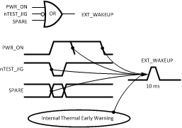 Figure 15. Wake-Up Functionality
Table 5. Wake-Up Functions
| WAKE-UP REGISTER BITS | REASON FOR WAKE-UP |
|---|---|
| WUP0 | SPARE |
| WUP1 | TEST_JIG |
| WUP2 | PWR_ON short pulse |
| WUP3 | PWR_ON long pulse |
| TSD_EW | TSD Early Warning |
8.5.1.1.6 Internal Thermal Shutdown Procedure
Thermal shutdown is build to generate early warning (typically 125°C) which triggers the EXT_WAKEUP for the processor acknowledge. When a thermal shutdown triggers (typical 160°C) the PMU resets the system until the device cools down.
8.5.1.1.7 Battery Switch and Backup Battery Charger
When backup battery is connected but the main battery has been removed or its supply voltage too low, the LP3972 uses the backup battery for generating LDO_RTC voltage. When Main Battery is available the battery FET switches over to the main battery for LDO_RTC voltage. When the main battery voltage is too low or removed nBATT_FLT is asserted. If no backup battery exists, the battery switch to backup can be switched off by nBU_BAT_EN bit. User can set the battery fault determination voltage and battery charger current via I2C-compatible interface. Enabling of backup battery charger can be done via serial interface (nBAT_CHG_EN) or external charger enable pin (nCHG_EN). The GPIO1/nCHG_EN pin is set as an external charger enable input by default.
8.5.1.1.8 General Purpose I/O Functionality (GPIO1 And GPIO2)
The LP3972 has 2 general purpose I/Os for system control. I2C-compatible interface is used for setting any of the pins to input, output or hi-Z mode. Inputs value can be read via serial interface (GPIO1,2 bits). The GPIO1/nCHG_EN pin functionality needs to be set to GPIO by serial interface register bit nEXTCHGEN (GPIO/CHG).
Table 6. GPIO1 Configuration Options
| CONTROLS | PORT FUNCTION | reg | batmonchg | |||
|---|---|---|---|---|---|---|
| GPIO<1> | GPIO<1> | Nextchgen_sel | bucen | GPIO1 | Gpin 1 | Function |
| X | X | 1 | 0 | Input = 0 | 0 | Enabled |
| X | X | 1 | 0 | Input = 1 | 0 | Not enabled |
| 1 | 0 | 1 | X | X | 0 | |
| X | X | X | 1 | X | Enabled | |
| 0 | 0 | 0 | X | HiZ | ||
| 1 | 0 | 0 | X | Input (dig)-> | Input | |
| 0 | 1 | 0 | X | Output = 0 | 0 | |
| 1 | 1 | 0 | X | Output = 1 | 0 | |
Table 7. GPIO2 Configuration Options
| GPIO<1> | GPIO<1> | GPIO_tstiob | GPIO2 | gpin2 |
|---|---|---|---|---|
| 0 | 0 | 1 | HiZ | 0 |
| 1 | 0 | 1 | Input (dig)-> | input |
| 0 | 1 | 1 | Output = 0 | 0 |
| 1 | 1 | 1 | Output = 1 | 0 |
The LP3972 has provision for two battery connections, the main battery VBAT and backup battery (see Figure 27).
The function of the battery switch is to connect power to the LDO_RTC from the appropriate battery, depending on conditions described as follows:
- If only the backup battery is applied, the switch automatically connects the LDO_RTC power to this battery.
- If only the main battery is applied, the switch automatically connects the LDO_RTC power to this battery.
- If both batteries are applied, and the main battery is sufficiently charged (VBAT > 3.1 V), the switch automatically connects the RTC LDO power to the main battery.
- As the main battery is discharged by use, the user is warned by a separate circuit called nBATT_FLT. Then if no action is taken to restore the charge on the main battery, and discharging is continued the battery switch protects the LDO_RTC by disconnecting from the main battery and connecting to the backup battery.
- The main battery voltage at which the LDO_RTC is switched from main to backup battery is 2.9 V typically.
- There is a hysteresis voltage in this switch operation so, the LDO_RTC is not reconnected to main battery until main battery voltage is greater than 3.1 V typically.
- Additionally, the user may wish to disable the battery switch, such as, in the case when only a main battery is used. This is accomplished by setting the no backup battery bit in the control register 8h’89 bit 7 NBUB. With this bit set to 1, the switching does not occur; that is, the LDO_RTC remains connected to the main battery even as it is discharged below the 2.9-V threshold.
8.5.1.1.9 Regulated Voltages OK
All the power domains have own register bit (X_OK) that processor can read via serial interface to be sure that enabled powers are OK (regulating). Note that these read only bits are only valid when regulators are settled (avoid reading these bits during voltage change or power up).
8.5.1.1.10 Thermal Management
There is a mode wherein all 6 comparators (flags) can be turned on via the enallflags control register bit. This mode allows the user to interrogate the device or system temperature under the set operating conditions. Thus, the rate of temperature change can also be estimated. The system may then negotiate for speed and power trade off, or deploy cooling maneuvers to optimize system performance. The enallflags bit needs enabled only when the bct<2:0> bits are read to conserve power.
NOTE
The thermal management flags have been verified functional. Presently these registers are accessible by factory only. If there is a demand for this function, the relevant register controls may be shifted into the user programmable bank; the temperature range and resolution of these flags, might also be refined or redefined.
8.5.1.1.11 Thermal Warning
Two of six low-power comparators, each consuming less than 1 µA, are always enabled to operate the T = 125°C warning flag with hysteresis. This allows continuous monitoring of a thermal-warning flag feature with very low power consumption.
8.5.1.1.12 LP3972 Thermal Flags Functional Diagram, Data from Initial Silicon
Figure 16 shows extra features from the thermal shutdown circuit:
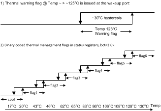 Figure 16. Thermal Shutdown Circuit Features
8.5.1.2 Initial Cold Start Power-On Sequence
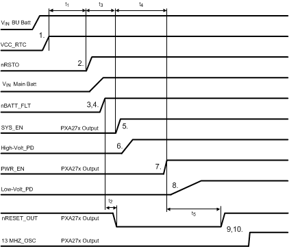
- The backup battery is connected to the PMU, power is applied to the backup battery pin, the LDO_RTC turns on and supplies a stable output voltage to the VCC_BATT pin of the Applications processor (initiating the power-on reset event) with nRSTO asserted from the LP3972 to the processor.
- nRSTO de-asserts after a minimum of 50 ms.
- The applications processor waits for the de-assertion of nBATT_FLT to indicate system power (VIN) is available.
- After system power (VIN) is applied, the LP3972 de-asserts nBATT_FLT. Note that BOTH nRSTO and nBATT_FLT need to be de-asserted before SYS_EN is enabled. The sequence of the two signals is independent of each other.
- The Applications processor asserts SYS_EN, the LP3972 enables the system high-voltage power supplies. The applications processor starts its countdown timer set to 125 ms.
- The LP3972 enables the high-voltage power supplies.
- LDO1 power for VCC_MVT (power for internal logic and I/O Blocks), BG (bandgap reference voltage), OSC13M (13-MHz oscillator voltage) and PLL enabled first, followed by others if delay is on.
- Countdown timer expires; the applications processor asserts PWR_EN to enable the low-voltage power supplies. The processor starts the countdown timer set to 125 ms period.
- The applications processor asserts PWR_EN (ext. pin or I2C), the LP3972 enables the low-voltage regulators.
- Countdown timer expires; if enabled power domains are OK (I2C read) the power-up sequence continues by enabling the 13-MHz oscillator of the processor and PLLs.
- The applications processor begins the execution of code.
See Power-On Timing Delays for more information.
8.5.1.3 Hardware Reset Sequence
Hardware reset initiates when the nRSTI signal is asserted (low). Upon assertion of nRST the processor enters hardware reset state. The LP3972 holds the nRST low long enough (50 ms typica) to allow the processor time to initiate the reset state.
8.5.1.4 Reset Sequence
- nRSTI is asserted.
- nRSTO is asserted and de-asserts after a minimum of 50 ms.
- The Applications processor waits for the de-assertion of nBATT_FLT to indicate system power (VIN) is available.
- After system power (VIN) is turned on, the LP3972 de-asserts nBATT_FLT.
- The applications processor asserts SYS_EN, the LP3972 enables the system high-voltage power supplies. The applications processor starts its countdown timer set to 125 ms.
- The LP3972 enables the high-voltage power supplies.
- Countdown timer expires; the applications processor asserts PWR_EN to enable the low-voltage power supplies. The processor starts the countdown timer set to 125 ms.
- The applications processor asserts PWR_EN, the LP3972 enables the low-voltage regulators.
- Countdown timer expires; if enabled power domains are OK (I2C read) the power-up sequence continues by enabling the 13-MHz oscillator of the processor and PLLs.
- The applications processor begins the execution of code.
8.5.2 I2C Compatible Interface
8.5.2.1 I2C Data Validity
The data on SDA line must be stable during the HIGH period of the clock signal (SCL). In other words, state of the data line can only be changed when CLK is LOW.
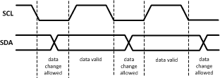 Figure 18. Data Validity
8.5.2.2 I2C Start And Stop Conditions
START and STOP bits classify the beginning and the end of the I2C session. START condition is defined as SDA signal transitioning from HIGH to LOW while SCL line is HIGH. STOP condition is defined as the SDA transitioning from LOW to HIGH while SCL is HIGH. The I2C master always generates START and STOP bits. The I2C bus is considered to be busy after START condition and free after STOP condition. During data transmission, I2C master can generate repeated START conditions. First START and repeated START conditions are equivalent, function-wise.
 Figure 19. Stop and Start Conditions
8.5.2.3 Transferring Data
Every byte put on the SDA line must be eight bits long, with the most significant bit (MSB) being transferred first. The number of bytes that can be transmitted per transfer is unrestricted. Each byte of data has to be followed by an acknowledge bit. The acknowledge related clock pulse is generated by the master. The transmitter releases the SDA line (HIGH) during the acknowledge clock pulse. The receiver must pull down the SDA line during the 9th clock pulse, signifying an acknowledge. A receiver which has been addressed must generate an acknowledge after each byte has been received.
After the START condition, a chip address is sent by the I2C master. This address is seven bits long followed by an eighth bit which is a data direction bit (R/W). The LP3972 address is 34h. For the eighth bit, a 0 indicates a WRITE and a1 indicates a READ. The second byte selects the register to which the data will be written. The third byte contains data to write to the selected register.
8.5.2.4 I2C Chip Address - 7h'34
Table 8. I2C Slave Address
| MSB | |||||||
| ADR6 Bit7 |
ADR5 Bit6 |
ADR4 Bit5 |
ADR3 Bit4 |
ADR2 Bit3 |
ADR1 Bit2 |
ADR0 Bit1 |
R/W
Bit0 |
| 0 | 1 | 1 | 0 | 1 | 0 | 0 | R/W |
8.5.2.4.1 Write Cycle
 Figure 20. Write Cycle
8.5.2.4.2 Read Cycle
When a READ function is to be accomplished, a WRITE function must precede the READ function as follows.

r = read (SDA = "1")
ack = acknowledge (SDA pulled down by either master or slave)
rs = repeated start
id = 34h (Chip Address)
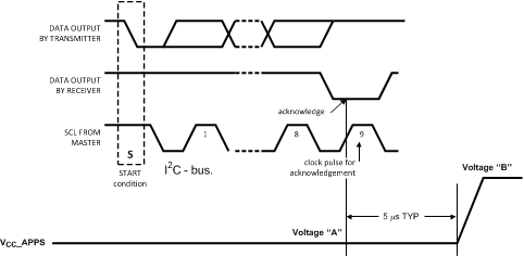 Figure 22. I2C DVM Timing For VCC_APPS (Buck1)
8.5.2.5 Multi-Byte I2C Command Sequence
To correctly function with the Monahan’s Power Management I2C the I2C serial interface of the device supports random register multi-byte command sequencing: During a multi-byte write the Master sends the start command followed by the device address, which is sent only once, followed by the 8-bit register address, then 8 bits of data. The I2C slave must then accept the next random register address followed by 8 bits of data and continue this process until the master sends a valid stop condition.
A typical multi-byte random register transfer is outlined in the following:
| Device Address |
Register A Address, Ach, Register A Data, Ach Register M Address, Ach, Register M Data, Ach Register X Address, Ach, Register X Data, Ach Register Z Address, Ach, Register Z Data, Ach, Stop |
NOTE
The PMIC is not required to see the I2C device address for each transaction. A, M, X, and Z are Random numbers.
 Figure 23. Multi-Byte I2C Command
8.5.2.6 Incremental Register I2C Command Sequence
The LP3972 supports address increment (burst mode). When there is a defined register address n data bytes can be sent, and the register address is incremented after each data byte has been sent. Address incrimination may be required for non XScale applications. User can define whether multi-byte (default) to random address or address incrimination will be used.
 Figure 24. Incremental Register I2C Command
8.6 Register Maps
Table 9. LP3972 Control Register
| REGISTER ADDRESS | REGISTER NAME | READ/WRITE | REGISTER DESCRIPTION |
|---|---|---|---|
| 8h’07 | SCR | R/W | System Control Register |
| 8h’10 | OVER1 | R/W | Output Voltage Enable Register 1 |
| 8h’11 | OVSR1 | R | Output Voltage Status Register 1 |
| 8h’12 | OVER2 | R/W | Output Voltage Enable Register 2 |
| 8h’13 | OVSR2 | R | Output Voltage Status Register 2 |
| 8h’20 | VCC1 | R/W | Voltage Change Control Register 1 |
| 8h’23 | ADTV1 | R/W | Buck1 Target Voltage 1 Register |
| 8h’24 | ADTV2 | R/W | Buck1 DVM Target Voltage 2 Register |
| 8h’25 | AVRC | R/W | VCC_APPS Voltage Ramp Control |
| 8h’26 | CDTC1 | W | Dummy Register |
| 8h’27 | CDTC2 | W | Dummy Register |
| 8h’29 | SDTV1 | R/W | LDO5 Target Voltage 1 |
| 8h’2A | SDTV2 | R/W | LDO5 Target Voltage 2 |
| 8h’32 | MDTV1 | R/W | LDO1 Target Voltage 1 Register |
| 8h’33 | MDTV2 | R/W | LDO1 Voltage 2 Register |
| 8h’39 | L2VCR | R/W | LDO2 Voltage Control Registers |
| 8h’3A | L34VCR | R/W | LDO3 & LDO4 Voltage Control Registers |
| 8h’80 | SCR1 | R/W | System Control Register 1 |
| 8h’81 | SCR2 | R/W | System Control Register 2 |
| 8h’82 | OEN3 | R/W | Output Voltage Enable Register 3 |
| 8h’83 | OSR3 | R/W | Output Voltage Status Register 3 |
| 8h’84 | LOER4 | R/W | Output Voltage Enable Register 3 |
| 8h’85 | B2TV | R/W | VCC_Buck2 Target Voltage |
| 8h’86 | B3TV | R/W | VCC_Buck3 Target Voltage |
| 8h’87 | B32RC | R/W | Buck 3:2 Voltage Ramp Control |
| 8h’88 | ISRA | R | Interrupt Status Register A |
| 8h’89 | BCCR | R/W | Backup Battery Charger Control Register |
| 8h’8E | II1RR | R | Internal 1 Revision Register |
| 8h’8F | II2RR | R | Internal 2 Revision Register |
8.6.1 Serial Interface Register Selection Codes
8.6.1.1 System Control Status Register
Register is an 8-bit register which specifies the control bits for the PMIC clocks. This register works in conjunction with the SYNC pin where an external clock PLL buffer operating at 13 MHz is synchronized with the oscillators of the buck converters.
8.6.1.1.1 System Control Register (SCR) 8h’07
| Bit | 7 | 6 | 5 | 4 | 3 | 2 | 1 | 0 |
|---|---|---|---|---|---|---|---|---|
| Designation | Reserved | CLK_SCL | ||||||
| Reset Value | 0 | 0 | 0 | 0 | 0 | 0 | 0 | 0 |
8.6.1.1.2 System Control Register (SCR) 8h’07 Definitions
| Bit | Access | Name | Description |
|---|---|---|---|
| 7-1 | — | — | Reserved |
| 0 | R/W | CLK_SCL | External Clock Select 0 = Internal oscillator clock for buck converters 1 = External 13-MHz oscillator clock for buck converters |
8.6.1.2 Output Voltage Enable Register 1
This register enables or disables the low voltage supplies LDO1 and Buck1. See details below.
8.6.1.2.1 Output Voltage Enable Register 1 (OVER1) 8h’10
| Bit | 7 | 6 | 5 | 4 | 3 | 2 | 1 | 0 |
|---|---|---|---|---|---|---|---|---|
| Designation | Reserved | S_EN | Reserved | A_EN | ||||
| Reset Value | 0 | 0 | 0 | 0 | 0 | 1 | 0 | 1 |
8.6.1.2.2 Output Voltage Enable Register 1 (OVER1) 8h’10 Definitions
| Bit | Access | Name | Description |
|---|---|---|---|
| 7-3 | — | — | Reserved |
| 2 | R/W | S_EN | VCC_SRAM (LDO5) Supply Output Enabled 0 = VCC_SRAM (LDO5) Supply Output Disabled 1 = VCC_SRAM (LDO5) Supply Output Enabled |
| 1 | — | — | Reserved |
| 0 | R/W | A_EN | VCC_APPS (Buck1) Supply Output Enabled 0 = VCC_APPS (Buck1) Supply Output Disabled 1 = VCC_APPS_ (Buck1) Supply Output Enabled |
8.6.1.3 Output Voltage Status Register
This 8-bit register is used to indicate the status of the low-voltage supplies. By polling each of the specify supplies is within its specified operating range.
8.6.1.3.1 Output Voltage Status Register 1 (OVSR1) 8h’11
| Bit | 7 | 6 | 5 | 4 | 3 | 2 | 1 | 0 |
|---|---|---|---|---|---|---|---|---|
| Designation | LP_OK | Reserved | S_OK | Reserved | A_OK | |||
| Reset Value | 0 | 0 | 0 | 0 | 0 | 0 | 0 | 0 |
8.6.1.3.2 Output Voltage Status Register 1 (OVSR1) 8h’11 Definitions
| Bit | Access | Name | Description |
|---|---|---|---|
| 7 | R | LP_OK | Low Voltage Supply Output Voltage Status 0 - VCC_APPS (Buck1) and VCC_SRAM (LDO5) output voltage < 90% of selected value 1 - VCC_APPS (Buck1) and VCC_SRAM (LDO5) output voltage > 90% of selected value |
| 6:3 | — | — | Reserved |
| 2 | R | S_OK | VCC-SRAM Supply Output Voltage Status 0 - VCC_SRAM (LDO5) output voltage < 90% of selected value 1 - VCC_SRAM (LDO5) output voltage > 90% of selected value |
| 1 | — | — | Reserved |
| 0 | R | A_OK | VCC_APPS Supply output Voltage Status 0 - VCC_APPS (Buck1) output voltage < 90% of selected value 1 - VCC_APPS (Buck1) output voltage > 90% of selected value |
8.6.1.4 Output Voltage Enable Register 2
This 8 bit output register enables and disables the output voltages on the LDOs 2,3,4 supplies.
8.6.1.4.1 Output Voltage Enable Register 2 (OVER2) 8h’12
8.6.1.4.2 Output Voltage Enable Register 2 (OVER2) 8h’12 Definitions
| BIT | ACCESS | NAME | DESCRIPTION |
|---|---|---|---|
| 7 | — | — | Reserved |
| 6 | — | — | Reserved |
| 5 | — | — | Reserved |
| 4 | R/W | LDO4_EN | LDO4 Output Voltage Enable 0 = LDO4 Supply Output Disabled, Default 1 = LDO4 Supply Output Enabled |
| 3 | R/W | LDO3_EN | LDO3 Output Voltage Enable 0 = LDO3 Supply Output Disabled, Default 1 = LDO3 Supply Output Enabled |
| 2 | R/W | LDO2_EN | LDO2 Output Voltage Enable 0 = LDO2 Supply Output Disabled, Default 1 = LDO2 Supply Output Enabled |
| 1 | — | — | Reserved |
| 0 | — | — | Reserved |
8.6.1.5 Output Voltage Status Register 2
8.6.1.5.1 Output Voltage Status Register 2 (OVSR2) 8h’13
| BIT | 7 | 6 | 5 | 4 | 3 | 2 | 1 | 0 |
|---|---|---|---|---|---|---|---|---|
| Designation | LDO_OK | N/A | N/A | LDO4_OK | LDO3_OK | LDO2_OK | N/A | N/A |
| Reset Value | 0 | 0 | 0 | 0 | 0 | 0 | 0 | 0 |
8.6.1.5.2 Output Voltage Status Register 2 (OVSR2) 8h’13 Definitions
| BIT | ACCESS | NAME | DESCRIPTION |
|---|---|---|---|
| 7 | R | LDO_OK | LDOs 2-4 Supply Output Voltage Status 0 - (LDOs 2-4) output voltage < 90% of selected value 1 - (LDOs 2-4) output voltage > 90% of selected value |
| 6 | — | — | Reserved |
| 5 | — | — | Reserved |
| 4 | R | LDO4_OK | LDO4 Output Voltage Status 0 - (VCC_LDO4) output voltage < 90% of selected value 1 - (VCC_LDO4) output voltage > 90% of selected value |
| 3 | R | LDO3_OK | LDO3 Output Voltage Status 0 - (VCC_LDO3) output voltage < 90% of selected value 1 - (VCC_LDO3) output voltage > 90% of selected value |
| 2 | R | LDO2_OK | LDO2 Output Voltage Status 0 - (VCC_LDO2) output voltage < 90% of selected value 1 - (VCC_LDO2) output voltage > 90% of selected value |
| 1 | — | — | Reserved |
| 0 | — | — | Reserved |
8.6.1.6 DVM Voltage Change Control Register 1
8.6.1.6.1 DVM Voltage Change Control Register 1 (VCC1) 8h’20
| BIT | 7 | 6 | 5 | 4 | 3 | 2 | 1 | 0 |
|---|---|---|---|---|---|---|---|---|
| Designation | MVS | MGO | SVS | SGO | Reserved | AVS | AGO | |
| Reset Value | 0 | 0 | 0 | 0 | 0 | 0 | 0 | 0 |
8.6.1.6.2 DVM Voltage Change Control Register 1 (VCC1) 8h’20 Definitions
| BIT | ACCESS | NAME | DESCRIPTION |
|---|---|---|---|
| 7 | R/W | MVS | VCC_MVT (LDO1) Voltage Select 0 - Change VCC_MVT Output Voltage to MDVT1 1 - Change VCC_MVT Output Voltage to MDVT2 |
| 6 | R/W | MGO | Start VCC_MVT (LDO1) Voltage Change 0 - Hold VCC_MVT Output Voltage at current Level 1 - Ramp VCC_MVT Output Voltage as selected by MVS |
| 5 | R/W | SVS | VCC_SRAM (LDO5) Voltage Select 0 - Change VCC_SRAM Output Voltage to SDTV1 1 - Change VCC_SRAM Output Voltage to SDTV2 |
| 4 | R/W | SGO | Start VCC_SRAM (LDO5) Voltage Change 0 - Hold VCC_SRAM Output Voltage at current Level 1 - Change VCC_SRAM Output Voltage as selected by SVS |
| 3:2 | — | — | Reserved |
| 1 | R/W | AVS | VCC_APPS (Buck1) Voltage Select 0 - Ramp VCC_APPS Output Voltage to ADVT1 1 - Ramp VCC_APPS Output Voltage to ADVT2 |
| 0 | R/W | AGO | Start VCC_APPS(Buck1) Voltage Change 0 - Hold VCC_APPS Output Voltage at current Level 1 - Ramp VCC_APPS Output Voltage as selected by AVS |
8.6.1.7 Buck1 (VCC_APPS) Voltage 1
8.6.1.7.1 Buck1 (VCC_APPS) Target Voltage 1 Register (ADTV1) 8h’23
8.6.1.7.2 Buck1 (VCC_apps) Target Voltage 1 Register (ADTV1) 8h’23 Definitions
| BIT | ACCESS | NAME | DESCRIPTION | |||
|---|---|---|---|---|---|---|
| 7:5 | — | — | Reserved | |||
| 4:0 | R/W | B1OV1 | Data Code
5h’0 5h’1 5h’2 5h’3 5h’4 5h’5 5h’6 5h’7 5h’8 5h’9 5h’A 5h’B 5h’C 5h’D 5h’E 5h’F |
Output Voltage
0.725 0.750 0.775 0.800 0.825 0.850 0.875 0.900 0.925 0.950 0.975 1.000 1.025 1.050 1.075 1.100 |
Data Code
5h’10 5h’11 5h’12 5h’13 5h’14 5h’15 5h’16 5h’17 5h’18 5h’19 5h’1A 5h'1B (default) 5h’1C 5h’1D 5h’1E 5h’1F |
Output Voltage
1.125 1.150 1.175 1.200 1.225 1.250 1.275 1.300 1.325 1.350 1.375 1.400 (default) 1.425 1.450 1.475 1.500 |
8.6.1.8 Buck1 (VCC_APPS) Target Voltage 2 Register
8.6.1.8.1 Buck1 (VCC_APPS) Target Voltage 2 Register (ADTV2) 8h’24
| BIT | 7 | 6 | 5 | 4 | 3 | 2 | 1 | 0 |
|---|---|---|---|---|---|---|---|---|
| Designation | Reserved | Buck1 Output Voltage (B1OV2) | ||||||
| Reset Value | 0 | 0 | 0 | 0 | 1 | 0 | 1 | 1 |
8.6.1.8.2 Buck1 (VCC_APPS) Target Voltage 2 Register (ADTV2) 8h’24 Definitions
| BIT | ACCESS | NAME | DESCRIPTION | |||
|---|---|---|---|---|---|---|
| 7:5 | — | — | Reserved | |||
| 4:0 | R/W | B1OV2 | Data Code
5h’0 5h’1 5h’2 5h’3 5h’4 5h’5 5h’6 5h’7 5h’8 5h’9 5h’A 5h’B 5h’C 5h’D 5h’E 5h’F |
Output Voltage
0.725 0.750 0.775 0.800 0.825 0.850 0.875 0.900 0.925 0.950 0.975 1.000 1.025 1.050 1.075 1.100 |
Data Code
5h’10 5h’11 5h’12 5h’13 5h’14 5h’15 5h’16 5h’17 5h’18 5h’19 5h’1A 5h’1B 5h’1C 5h’1D 5h’1E 5h’1F |
Output Voltage
1.125 1.150 1.175 1.200 1.225 1.250 1.275 1.300 1.325 1.350 1.375 1.400 1.425 1.450 1.475 1.500 |
8.6.1.9 Buck1 (VCC_APPS) Voltage Ramp Control Register
8.6.1.9.1 Buck1 (VCC_APPS) Voltage Ramp Control Register (AVRC) 8h’25
| BIT | 7 | 6 | 5 | 4 | 3 | 2 | 1 | 0 |
|---|---|---|---|---|---|---|---|---|
| Designation | Reserved | Ramp Rate (B1RR) | ||||||
| Reset Value | 0 | 0 | 0 | 0 | 1 | 0 | 1 | 0 |
8.6.1.9.2 Buck1 (VCC_APPS) Voltage Ramp Control Register (AVRC) 8h’25 Definitions
| BIT | ACCESS | NAME | DESCRIPTION | |
|---|---|---|---|---|
| 7:5 | — | — | Reserved | |
| 4:0 | R/W | B1RR | DVM Ramp Speed | |
| Data Code
5h’0 5h’1 5h’2 5h’3 5h’4 5h’5 5h’6 5h’7 5h’8 5h’9 5h’A 4h’B-4h’1F |
Ramp Rate (mV/us)
Instant 1 2 3 4 5 6 7 8 9 10 (default) Reserved |
|||
8.6.1.10 VCC_comm Target Voltage 1 Dummy Register (CDTV1)
8.6.1.10.1 VCC_comm Target Voltage 1 Dummy Register (CDTV1) 8h’26 Write Only(1)
| BIT | 7 | 6 | 5 | 4 | 3 | 2 | 1 | 0 |
|---|---|---|---|---|---|---|---|---|
| Designation | Reserved | Output Voltage | ||||||
| Reset Value | 0 | 0 | 0 | 0 | 0 | 0 | 0 | 0 |
8.6.1.11 VCC_COMM Target Voltage 2 Dummy Register (CDTV2)
8.6.1.11.1 VCC_COMM Target Voltage 2 Dummy Register (CDTV2) 8h’27 Write Only(1)
| BIT | 7 | 6 | 5 | 4 | 3 | 2 | 1 | 0 |
|---|---|---|---|---|---|---|---|---|
| Designation | Reserved | Output Voltage | ||||||
| Reset Value | 0 | 0 | 0 | 0 | 0 | 0 | 0 | 0 |
This is a variable voltage supply to the internal SRAM of the application processor.
8.6.1.12 LDO5 (VCC_SRAM) Target Voltage 1 Register
8.6.1.12.1 LDO5 (VCC_SRAM) Target Voltage 1 Register (SDTV1) 8h'29
8.6.1.12.2 LDO5 (VCC_SRAM) Target Voltage 1 Register (SDTV1) 8h’29 Definitions
| BIT | ACCESS | NAME | DESCRIPTION | |||
|---|---|---|---|---|---|---|
| 7:5 | — | — | Reserved | |||
| 4:0 | R/W | B1OV | Data Code
5h’0 5h’1 5h’2 5h’3 5h’4 5h’5 5h’6 5h’7 5h’8 5h’9 5h’A 5h’B 5h’C 5h’D 5h’E 5h’F |
Output Voltage
— — — — — 0.850 0.875 0.900 0.925 0.950 0.975 1.000 1.025 1.050 1.075 1.100 |
Data Code
5h’10 5h’11 5h’12 5h’13 5h’14 5h’15 5h’16 5h’17 5h’18 5h’19 5h’1A 5h’1B (default) 5h’1C 5h’1D 5h’1E 5h’1F |
Output Voltage
1.125 1.150 1.175 1.200 1.225 1.250 1.275 1.300 1.325 1.350 1.375 1.400 (default) 1.425 1.450 1.475 1.500 |
8.6.1.13 LDO5 (VCC_SRAM) Target Voltage 2 Register
8.6.1.13.1 LDO5 (VCC_SRAM) Target Voltage 2 Register (SDTV2) 8h’2A
| BIT | 7 | 6 | 5 | 4 | 3 | 2 | 1 | 0 |
|---|---|---|---|---|---|---|---|---|
| Designation | Reserved | LDO 5 Output Voltage (L5OV) | ||||||
| Reset Value | 0 | 0 | 0 | 0 | 1 | 0 | 1 | 1 |
8.6.1.13.2 LDO5 (VCC_SRAM) Target Voltage 2 Register (SDTV2) 8h’2A Definitions
| BIT | ACCESS | NAME | DESCRIPTION | |||
|---|---|---|---|---|---|---|
| 7:5 | — | — | Reserved | |||
| 4:0 | R/W | B1OV | Data Code
5h’0 5h’1 5h’2 5h’3 5h’4 5h’5 5h’6 5h’7 5h’8 5h’9 5h’A 5h’B 5h’C 5h’D 5h’E 5h’F |
Output Voltage
— — — — — 0.850 0.875 0.900 0.925 0.950 0.975 1.000 1.025 1.050 1.075 1.100 |
Data Code
5h’10 5h’11 5h’12 5h’13 5h’14 5h’15 5h’16 5h’17 5h’18 5h’19 5h’1A 5h’1B 5h’1C 5h’1D 5h’1E 5h’1F |
Output Voltage
1.125 1.150 1.175 1.200 1.225 1.250 1.275 1.300 1.325 1.350 1.375 1.400 1.425 1.450 1.475 1.500 |
VCC_MVT is low tolerance regulated power supply for the application processor ring oscillator and logic for communicating to the LP3972. VCC_MVT is enabled when SYS_EN is asserted and disabled when SYS_EN is deasserted.
8.6.1.14 LDO1 (VCC_MVT) Target Voltage 1 Register (MDTV1)
8.6.1.14.1 LDO1 (VCC_MVT) Target Voltage 1 Register (MDTV1) 8h’32
8.6.1.14.2 LDO1 (VCC_MVT) Target Voltage 1 Register (MDTV1) 8h’32 Definitions
| BIT | ACCESS | NAME | DESCRIPTION | ||
|---|---|---|---|---|---|
| 7:5 | — | — | Reserved | ||
| 4:0 | R/W | L1OV | Data Code
5h’0 5h’1 5h’2 5h’3 5h’4 (default) 5h’5 5h’6 5h’7 5h’8 5h’9 5h’A 5h’B 5h’C 5h’D-5h’F |
Output Voltage
1.700 1.725 1.750 1.775 1.800 (default) 1.825 1.850 1.875 1.900 1.925 1.950 1.975 2.000 Reserved |
Notes: |
8.6.1.15 LDO1 (VCC_MVT) Target Voltage 2 Register
8.6.1.15.1 LDO1 (VCC_MVT) Target Voltage 2 Register (MDTV2) 8h’33
| BIT | 7 | 6 | 5 | 4 | 3 | 2 | 1 | 0 |
|---|---|---|---|---|---|---|---|---|
| Designation | Reserved | Output Voltage (OV) | ||||||
| Reset Value | 0 | 0 | 0 | 0 | 1 | 0 | 1 | 1 |
8.6.1.15.2 LDO1 (VCC_MVT) Target Voltage 2 Register (MDTV2) 8h’33 Definitions
| BIT | ACCESS | NAME | DESCRIPTION | ||
|---|---|---|---|---|---|
| 7:5 | — | — | Reserved | ||
| 4:0 | R/W | L1OV | Data Code
5h’0 5h’1 5h’2 5h’3 5h’4 (default) 5h’5 5h’6 5h’7 5h’8 5h’9 5h’A 5h’B 5h’C 5h’D-5h’F |
Output Voltage
1.700 1.725 1.750 1.775 1.800 (default) 1.825 1.850 1.875 1.900 1.925 1.950 1.975 2.000 Reserved |
Notes: |
8.6.1.16 LDO2 Voltage Control Register (L12VCR)
8.6.1.16.1 LDO2 Voltage Control Register (L12VCR) 8h’39
8.6.1.16.2 LDO2 Voltage Control Register (L12VCR) 8h’39 Definitions
| BIT | ACCESS | NAME | DESCRIPTION | |
|---|---|---|---|---|
| 7:4 | R/W | L2OV | Data Code
4h’0 (default) 4h’1 4h’2 4h’3 4h’4 4h’5 4h’6 4h’7 4h’8 4h’9 4h’A 4h’B 4h’C 4h’D 4h’E 4h’F |
Output Voltage
1.8 (Default) 1.9 2.0 2.1 2.2 2.3 2.4 2.5 2.6 2.7 2.8 2.9 3.0 3.1 3.2 3.3 |
| 3:0 | — | — | Reserved | |
8.6.1.17 LDO4 – LDO3 Voltage Control Register (L34VCR)
8.6.1.17.1 LDO4 – LDO3 Voltage Control Register (L34VCR) 8h’3A
8.6.1.17.2 LDO4 – LDO3 Voltage Control Register (L34VCR) 8h’3A Definitions
| BIT | ACCESS | NAME | DESCRIPTION | |
|---|---|---|---|---|
| 7:4 | R/W | L4OV | Data Code
4h’0 4h’1 4h’2 4h’3 4h’4 4h’5 4h’6 4h’7 4h’8 4h’9 4h’A 4h’B 4h’C 4h’D 4h’E (default0 4h’F |
Output Voltage
1.00 1.05 1.10 1.15 1.20 1.25 1.30 1.35 1.40 1.50 1.80 1.90 2.50 2.80 3.00 (default) (Default) 3.30 |
| 3:0 | R/W | L3OV | Data Code
4h’0 4h’1 4h’2 4h’3 4h’4 4h’5 4h’6 4h’7 4h’8 4h’9 4h’A 4h’B 4h’C (default) 4h’D 4h’E 4h’F |
Output Voltage
1.8 1.9 2.0 2.1 2.2 2.3 2.4 2.5 2.6 2.7 2.8 2.9 3.0 (Default) 3.1 3.2 3.3 |
8.6.2 TI-Defined Control and Status Registers
8.6.2.1 System Control Register 1 (SCR1)
8.6.2.1.1 System Control Register 1 (SCR1) 8h’80
8.6.2.1.2 System Control Register 1 (SCR1) 8h’80 Definitions
| BIT | ACCESS | NAME | DESCRIPTION | ||
|---|---|---|---|---|---|
| 7 | R/W | BPSEN | Bypass System enable safety Lock. Prevents activation of PWR_EN when SYS_EN is low. 0 = PWR_EN "AND" with SYS_EN signal, Default 1 = PWR_EN independent of SYS_EN |
||
| 6:5 | R/W | SENDL | Delay time for High Voltage Power Domains LDO2, LDO3, LDO4, Buck2, and Buck3 after activation of SYS_EN. VCC_LDO1 has no delay. | ||
| Data Code
2h’0 2h’1 2h’2 2h’3 |
Delay (ms)
0.0 0.5 1 (Default) 1.4 |
||||
| 4 | R/W | FPWM3 | Buck3 PWM/PFM Mode select 0 - Auto Switch between PFM and PWM operation 1 - PWM Mode Only does not switch to PFM |
||
| 3 | R/W | FPWM2 | Buck2 PWM/PFM Mode select 0 - Auto Switch between PFM and PWM operation 1 - PWM Mode Only does not switch to PFM |
||
| 2 | R/W | FPWM1 | Buck1 PWM/PFM Mode select 0 - Auto Switch between PFM and PWM operation 1 - PWM Mode Only does not switch to PFM |
||
| 1 | R | BK_SLOMOD | Buck Spread Spectrum Modulation Bucks 1-3 0 = 10 kHz triangular wave spread spectrum modulation 1 = 2 kHz triangular wave spread spectrum modulation |
||
| 0 | R | BK_SSEN | Spread spectrum function Bucks 1-3 0 = SS Output Disabled 1 = SS Output Enabled |
||
8.6.2.2 System Control Register 2 (SCR2)
8.6.2.2.1 System Control Register 2 (SCR2) 8h’81
| BIT | 7 | 6 | 5(1) | 4 | 3 | 2 | 1 | 0 |
|---|---|---|---|---|---|---|---|---|
| Designation | BBCS | SHBU | BPTR | WUP3 | GPIO2 | GPIO1 | ||
| 1 | 0 | 1 | 1 | 0 | 0 | 1 | 0 | |
8.6.2.2.2 System Control Register 2 (SCR2) 8h’81 Definitions
| BIT | ACCESS | NAME | DESCRIPTION | ||
|---|---|---|---|---|---|
| 7 | R/W | BBCS | Sets GPIO1 as control input for backup battery charger 0 - Backup battery Charger GPIO Disabled 1 - Backup battery Charger GPIO Pin Enabled |
||
| 6 | R/W | SHBU | Shut down backup battery to prevent battery drain during shipping 0 = Backup Battery Enabled 1 = Backup battery Disabled |
||
| 5 | R/W | BPTR | Bypass LDO_RTC Output Voltage to LDO3 Output Voltage Tracking 0 - LDO_RTC3 Tracking enabled 1 - LDO_RTC3 Tracking disabled, Default |
||
| 4 | R/W | WUP3 | Spare Wake-up control input 0 - Active High 1 - Active Low |
||
| 3:2 | R/W | GPIO2 | Configure direction and output sense of GPIO2 Pin | ||
| Data Code
2h’00 2h’01 2h’02 2h’03 |
GPIO2
Hi-Z Output Low Input Output high |
||||
| 1:0 | R/W | GPIO1 | Configure direction and output sense of GPIO1 Pin | ||
| Data Code
2h’00 2h’01 2h’02 2h’03 |
GPIO1
Hi-Z Output Low Input Output high |
||||
8.6.2.3 Output Enable 3 Register (OEN3) 8h’82
8.6.2.4 Output Enable 3 Register (OEN3) 8h’82 Definitions
| BIT | ACCESS | NAME | DESCRIPTION |
|---|---|---|---|
| 7:5 | — | — | Reserved |
| 4 | R/W | B3EN | VCC_Buck3 Supply Output Enabled 0 = VCC_Buck3 Supply Output Disabled 1 = VCC_Buck3 Supply Output Enabled, Default |
| 3 | R/W | ENFLAG | Enable for Temperature Flags (BCT) 0 = Temperature Flag Disabled 1 = Temperature Flag Enabled |
| 2 | R/W | B2EN | VCC_Buck2 Supply Output Enabled 0 = VCC_Buck2 Supply Output Disabled 1 = VCC_Buck2 Supply Output Enabled, Default |
| 1 | — | — | Reserved |
| 0 | R/W | L1EN | LDO1 (MVT)Output Voltage Enable 0 = LDO1 Supply Output Disabled 1 = LDO1 Supply Output Enabled, Default |
8.6.2.5 Status Register 3 (OSR3) 8h’83
| BIT | 7 | 6 | 5 | 4 | 3 | 2 | 1 | 0 |
|---|---|---|---|---|---|---|---|---|
| Designation | BT_OK | B3_OK | B2_OK | LDO1_OK | Reserved | BCT2 | BCT1 | BCT0 |
| Reset Value | 0 | 0 | 0 | 0 | 0 | 0 | 0 | 0 |
8.6.2.6 Status Register 3 (OSR3) Definitions 8h’83
| BIT | ACCESS | NAME | DESCRIPTION | ||
|---|---|---|---|---|---|
| 7 | R | BT_OK | Bucks 2-3 Supply Output Voltage Status 0 - (Bucks 1-3) output voltage < 90% Default value 1 - (Bucsk 1-3) output voltage > 90% Default value |
||
| 6 | R | B3_OK | Buck3 Supply Output Voltage Status 0 - (Buck3) output voltage < 90% Default value 1 - (Buck3) output voltage > 90% Default value |
||
| 5 | R | B2_OK | Buck2 Supply Output Voltage Status 0 - (Buck2) output voltage < 90% Default value 1 - (Buck2) output voltage > 90% Default value |
||
| 4 | R | LDO1_OK | LDO1 Output Voltage Status 0 - (VCC_LDO1) output voltage < 90% of selected value 1 - (VCC_LDO1) output voltage > 90% of selected value |
||
| 3 | — | — | Reserved | ||
| 2:0 | R | BCT | Binary coded thermal management flag status register | ||
| Data Code 000 001 010 011 100 101 110 111 |
Temperature
Ascending °C 40 60 80 100 120 140 160 Reserved |
||||
8.6.2.7 Logic Output Enable Register (LOER) 8h’84
8.6.2.8 Logic Output Enable Register (LOER) Definitions 8h’84
| BIT | ACCESS | NAME | DESCRIPTION |
|---|---|---|---|
| 7 | — | — | Reserved |
| 6 | R/W | B3ENC | Connects Buck3 enable to SYS_EN or PWR_EN Logic Control pin 0 - Buck3 enable connected to PWR_EN 1 - Buck3 enable connected to SYS_EN, Default |
| 5 | R/W | B2ENC | Connects Buck2 enable to SYS_EN or PWR_EN Logic Control pin 0 - Buck2 enable connected to PWR_EN 1 - Buck2 enable connected to SYS_EN, Default |
| 4 | R/W | B1ENC | Connects Buck1 enable to SYS_EN or PWR_EN Logic Control pin 0 - Buck1 enable connected to PWR_EN, Default 1 - Buck1 enable connected to SYS_EN |
| 3 | R/W | L5EC | Connects LDO5 enable to SYS_EN or PWR_EN Logic Control pin 0 - LDO5 enable connected to PWR_EN, Default 1 - LDO5 enable connected to SYS_EN |
| 2 | R/W | L4EC | Connects LDO4 enable to SYS_EN or PWR_EN Logic Control pin 0 - LDO4 enable connected to PWR_EN 1 - LDO4 enable connected to SYS_EN, Default |
| 1 | R/W | L3EC | Connects LDO3 enable to SYS_EN or PWR_EN Logic Control pin 0 - LDO3 enable connected to PWR_EN 1 - LDO3 enable connected to SYS_EN, Default |
| 0 | R/W | L2EC | Connects LDO2 enable to SYS_EN or PWR_EN Logic Control pin 0 - LDO2 enable connected to PWR_EN 1 - LDO2 enable connected to SYS_EN, Default |
8.6.2.9 VCC_BUCK2 Target Voltage Register (B2TV) 8h’85
8.6.2.10 VCC_BUCK2 Target Voltage Register (B2TV) 8h’85 Definitions
| Bit | Access | Name | Description | |||
|---|---|---|---|---|---|---|
| 7:5 | — | Reserved | ||||
| 4:0 | R/W | B2OV | Output Voltage | |||
| Data Code
5h’01 5h’02 5h’03 5h’04 5h’05 5h’06 5h’07 5h’08 5h’09 5h’0A 5h’0B 5h’0C |
(V)
0.80 0.85 0.90 0.95 1.00 1.05 1.10 1.15 1.20 1.25 1.30 1.35 |
Data Code
5h’0D 5h’0E 5h’0F 5h’10 5h’11 5h’12 5h’13 5h’14 5h’15 5h’16 5h’17 5h’18 5h’19 (default) |
(V)
1.40 1.45 1.50 1.55 1.60 1.65 1.70 1.80 1.90 2.50 2.80 3.00 3.30 (default) |
|||
8.6.2.11 BUCK3 Target Voltage Register (B3TV) 8h’86
8.6.2.12 BUCK3 Target Voltage Register (B3TV) 8h’86 Definitions
| Bit | Access | Name | Description | ||||
|---|---|---|---|---|---|---|---|
| 7:5 | — | Reserved | |||||
| 4:0 | R/W | B3OV | Output Voltage | ||||
| Data Code
5h’01 5h’02 5h’03 5h’04 5h’05 5h’06 5h’07 5h’08 5h’09 5h’0A 5h’0B 5h’0C |
(V)
0.80 0.85 0.90 0.95 1.00 1.05 1.10 1.15 1.20 1.25 1.30 1.35 |
Data Code
5h’0D 5h’0E 5h’0F 5h’11 5h’12 5h’13 5h’14 (default) 5h’15 5h’16 5h’17 5h’18 5h’19 |
(V)
1.40 1.45 1.50 1.60 1.65 1.70 1.80 (default) 1.90 2.50 2.80 3.00 3.30 |
Default |
|||
8.6.2.13 VCC_BUCK3:2 Voltage Ramp Control Register (B32RC)
8.6.2.13.1 VCC_BUCK3:2 Voltage Ramp Control Register (B32RC) 8h’87
| Bit | 7 | 6 | 5 | 4 | 3 | 2 | 1 | 0 |
|---|---|---|---|---|---|---|---|---|
| Designation | Ramp Rate (B3RR) | Ramp Rate (B2RR) | ||||||
| Reset Value | 1 | 0 | 1 | 0 | 1 | 0 | 1 | 0 |
8.6.2.13.2 Buck3:2 Voltage Ramp Control Register (B3RC) 8h’87 Definitions
| Bit | Access | Name | Description | |
|---|---|---|---|---|
| 7:4 | R/W | B3RR | Data Code
4h’0 4h’1 4h’2 4h’3 4h’4 4h’5 4h’6 4h’7 4h’8 4h’9 4h’A |
Ramp Rate mV/µS
Instant 1 2 3 4 5 6 7 8 9 10 |
| 3:0 | R/W | B2RR | Data Code
4h’0 4h’1 4h’2 4h’3 4h’4 4h’5 4h’6 4h’7 4h’8 4h’9 4h’A (default) |
Ramp Rate mV/µS
Instant 1 2 3 4 5 6 7 8 9 10 (default) |
8.6.2.14 Interrupt Status Register ISRA
This register specifies the status bits for the interrupts generated by the LP3972 device.
8.6.2.14.1 Interrupt Status Register ISRA 8h’88
| Bit | 7 | 6 | 5 | 4 | 3 | 2 | 1 | 0 |
|---|---|---|---|---|---|---|---|---|
| Designation | Reserved | T125 | GPI2 | GPI1 | WUP3 | WUP2 | WUPT | WUPS |
| Reset Value | 0 | 0 | 0 | 0 | 0 | 0 | 0 | 0 |
8.6.2.14.2 Interrupt Status Register ISRA 8h’88 Definitions
| Bit | Access | Name | Description |
|---|---|---|---|
| 7 | — | — | Reserved |
| 6 | R | T125 | Status bit for thermal warning PMIC T>125°C 0 = PMIC Temp. < 125°C 1 = PMIC Temp. > 125°C |
| 5 | R | GPI2 | Status bit for the input read in from GPIO 2 when set as Input 0 = GPI2 Logic Low 1 = GPI2 Logic High |
| 4 | R | GPI1 | Status bit for the input read in from GPIO 1 when set as Input 0 = GPI1 Logic Low 1 = GPI1 Logic High |
| 3 | R | WUP3 | PWR_ON Pin long pulse wake-up status 0 = No wake-up event 1 = Long pulse wake-up event |
| 2 | R | WUP2 | PWR_ON Pin Short pulse wake-up Status 0 = No wake-up event 1 = Short pulse wake-up event |
| 1 | R | WUPT | TEST_JIG Pin wake-up Status 0 = No wake-up event 1 = Wake-up event |
| 0 | R | WUPS | SPARE pin wake-up status 0 = No wake-up event 1 = Wake-up event |
8.6.2.15 Backup Battery Charger Control Register (BCCR)
This register specifies the status of the main battery supply (NBUB bit).
8.6.2.15.1 Backup Battery Charger Control Register (BCCR) 8h’89
8.6.2.15.2 Backup Battery Charger Control Register (BCCR) 8h’89 Definitions
| Bit | Access | Name | Description | |||
|---|---|---|---|---|---|---|
| 7 | R/W | NBUB | No backup battery default setting. Logic does not allow switch-over to backup battery. 0 = Backup Battery Enabled, Default 1 = Backup Battery Disabled |
|||
| 6 | R/W | CNBFL | Control for nBATT_FLT output signal 0 = nBATT_FLT Enabled 1 = nBATT_FLT Disabled |
|||
| 5:3 | R/W | BFLT | nBATT_FLT monitors the battery voltage and can be set to the Assert voltages listed below. | |||
| Data Code
3h’01 3h’02 3h’03 3h’04 3h’05 |
Asserted
2.6 2.8 (default) 3.0 3.2 3.4 |
De-Asserted
2.8 3.0 (Default) 3.2 3.4 3.6 |
||||
| 2 | R/W | BUCEN | Enables backup battery charger 0 = Backup Battery Charger Disabled 1 = Backup Battery Charger Enabled |
|||
| 1:0 | R/W | IBUC | Charger current setting for backup battery | |||
| Data Code
2h’00 2h’01 (default) 2h’02 2h’03 |
BU Charger I (µA)
260 190 (Default) 325 390 |
|||||
8.6.2.16 Marvell PXA Internal 1 Revision Register (II1RR) 8h’8E
| Bit | 7 | 6 | 5 | 4 | 3 | 2 | 1 | 0 |
|---|---|---|---|---|---|---|---|---|
| Designation | II1RR | |||||||
| Reset Value | 0 | 0 | 0 | 0 | 0 | 0 | 0 | 0 |
8.6.2.17 Marvell PXA Internal 1 Revision Register (II1RR) (Ii1rr) 8h’8E Definitions
| Bit | Access | Name | Description |
|---|---|---|---|
| 7:0 | R | II1RR | Intel internal usage register for revision information. |
8.6.2.18 Marvell PXA Internal 2 Revision Register (II1RR) 8h’8F
| Bit | 7 | 6 | 5 | 4 | 3 | 2 | 1 | 0 |
|---|---|---|---|---|---|---|---|---|
| Designation | II2RR | |||||||
| Reset Value | 0 | 0 | 0 | 0 | 0 | 0 | 0 | 0 |
8.6.2.19 Marvell PXA Internal 2 Revision Register (II1RR) 8h’8F Definitions
| Bit | Access | Name | Description |
|---|---|---|---|
| 7:0 | R | II2RR | Intel internal usage register for revision information. |
8.6.2.20 Register Programming Examples
8.6.2.20.1 Example 1: Start-of-Day (SOD) Sequence
| PMIC Register Address | PMIC Register Name | Register Data | Description |
|---|---|---|---|
| 8h’23 | ADTVI | 00011011 | Sets the SOD VCC_APPS voltage |
| 8h’29 | SDTV1 | 00011011 | Sets the SOD VCC_SRAM voltage |
| 8h’10 | OVER1 | 00000111 | Enables VCC_SRAM and VCC_APPS to their programmed values. |
SODl multi-byte random register transfer is shown in Figure 25:
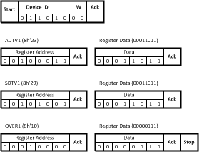 Figure 25. SOD Multi-Byte Random Register Transfer
| Device Address |
Register A Address, Ach, Register A Data, Ach Register M Address, Ach, Register M Data, Ach Register X Address, Ach, Register X Data, Ach Register Z Address, Ach, Register Z Data, Ach, Stop |
8.6.2.20.2 Example 2: Voltage Change Sequence
| PMIC Register Address | PMIC Register Name | Register Data | Description |
|---|---|---|---|
| 8h’24 | ADTV2 | 00010111 | Sets the VCCAPPS_ target voltage 2 to 1.3 V. |
| 8h’2A | SDTV2 | 00001111 | Sets the VCC_SRAM target voltage 2 to 1.1 V. |
| 8h’20 | VCC1 | 00110011 | Enables VCC_SRAM and VCC_APPS to change to their programmed target values. |
8.6.2.20.3 I2C Data Exchange Between Master and Slave Device
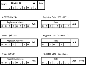 Figure 26. Master and Slave Data Exchange