SNVS468L September 2006 – November 2015 LP3972
PRODUCTION DATA.
- 1 Features
- 2 Applications
- 3 Description
- 4 Revision History
- 5 Device Comparison Tables
- 6 Pin Configuration and Functions
-
7 Specifications
- 7.1 Absolute Maximum Ratings
- 7.2 ESD Ratings
- 7.3 Recommended Operating Conditions
- 7.4 Thermal Information
- 7.5 Electrical Characteristics
- 7.6 Electrical Characteristics: LDO RTC
- 7.7 Electrical Characteristics: LDOs 1 to 5
- 7.8 Electrical Characteristics: Buck Converters SW1, SW2, SW3
- 7.9 Electrical Characteristics: Backup Charger
- 7.10 Electrical Characteristics: I2C Compatible Serial Interface (SDA and SCL)
- 7.11 Logic Inputs and Outputs DC Operating Conditions
- 7.12 I2C Compatible Serial Interface Timing Requirements (SDA and SCL)
- 7.13 Power-On Timing Delays
- 7.14 Typical Characteristics
-
8 Detailed Description
- 8.1 Overview
- 8.2 Functional Block Diagram
- 8.3 Feature Description
- 8.4 Device Functional Modes
- 8.5
Programming
- 8.5.1
LP3972 Reset Sequence
- 8.5.1.1
LP3972 Controls
- 8.5.1.1.1 Digital Interface Control Signals
- 8.5.1.1.2 Power Domain Enables
- 8.5.1.1.3 Power Domains Sequencing (Delay)
- 8.5.1.1.4 Power Supply Enable
- 8.5.1.1.5 Wake-up Functionality (PWR_ON, NTEST_JIG, SPARE and EXT_WAKEUP)
- 8.5.1.1.6 Internal Thermal Shutdown Procedure
- 8.5.1.1.7 Battery Switch and Backup Battery Charger
- 8.5.1.1.8 General Purpose I/O Functionality (GPIO1 And GPIO2)
- 8.5.1.1.9 Regulated Voltages OK
- 8.5.1.1.10 Thermal Management
- 8.5.1.1.11 Thermal Warning
- 8.5.1.1.12 LP3972 Thermal Flags Functional Diagram, Data from Initial Silicon
- 8.5.1.2 Initial Cold Start Power-On Sequence
- 8.5.1.3 Hardware Reset Sequence
- 8.5.1.4 Reset Sequence
- 8.5.1.1
LP3972 Controls
- 8.5.2 I2C Compatible Interface
- 8.5.1
LP3972 Reset Sequence
- 8.6
Register Maps
- 8.6.1
Serial Interface Register Selection Codes
- 8.6.1.1 System Control Status Register
- 8.6.1.2 Output Voltage Enable Register 1
- 8.6.1.3 Output Voltage Status Register
- 8.6.1.4 Output Voltage Enable Register 2
- 8.6.1.5 Output Voltage Status Register 2
- 8.6.1.6 DVM Voltage Change Control Register 1
- 8.6.1.7 Buck1 (VCC_APPS) Voltage 1
- 8.6.1.8 Buck1 (VCC_APPS) Target Voltage 2 Register
- 8.6.1.9 Buck1 (VCC_APPS) Voltage Ramp Control Register
- 8.6.1.10 VCC_comm Target Voltage 1 Dummy Register (CDTV1)
- 8.6.1.11 VCC_COMM Target Voltage 2 Dummy Register (CDTV2)
- 8.6.1.12 LDO5 (VCC_SRAM) Target Voltage 1 Register
- 8.6.1.13 LDO5 (VCC_SRAM) Target Voltage 2 Register
- 8.6.1.14 LDO1 (VCC_MVT) Target Voltage 1 Register (MDTV1)
- 8.6.1.15 LDO1 (VCC_MVT) Target Voltage 2 Register
- 8.6.1.16 LDO2 Voltage Control Register (L12VCR)
- 8.6.1.17 LDO4 - LDO3 Voltage Control Register (L34VCR)
- 8.6.2
TI-Defined Control and Status Registers
- 8.6.2.1 System Control Register 1 (SCR1)
- 8.6.2.2 System Control Register 2 (SCR2)
- 8.6.2.3 Output Enable 3 Register (OEN3) 8h’82
- 8.6.2.4 Output Enable 3 Register (OEN3) 8h’82 Definitions
- 8.6.2.5 Status Register 3 (OSR3) 8h’83
- 8.6.2.6 Status Register 3 (OSR3) Definitions 8h’83
- 8.6.2.7 Logic Output Enable Register (LOER) 8h’84
- 8.6.2.8 Logic Output Enable Register (LOER) Definitions 8h’84
- 8.6.2.9 VCC_BUCK2 Target Voltage Register (B2TV) 8h’85
- 8.6.2.10 VCC_BUCK2 Target Voltage Register (B2TV) 8h’85 Definitions
- 8.6.2.11 BUCK3 Target Voltage Register (B3TV) 8h’86
- 8.6.2.12 BUCK3 Target Voltage Register (B3TV) 8h’86 Definitions
- 8.6.2.13 VCC_BUCK3:2 Voltage Ramp Control Register (B32RC)
- 8.6.2.14 Interrupt Status Register ISRA
- 8.6.2.15 Backup Battery Charger Control Register (BCCR)
- 8.6.2.16 Marvell PXA Internal 1 Revision Register (II1RR) 8h’8E
- 8.6.2.17 Marvell PXA Internal 1 Revision Register (II1RR) (Ii1rr) 8h’8E Definitions
- 8.6.2.18 Marvell PXA Internal 2 Revision Register (II1RR) 8h’8F
- 8.6.2.19 Marvell PXA Internal 2 Revision Register (II1RR) 8h’8F Definitions
- 8.6.2.20 Register Programming Examples
- 8.6.1
Serial Interface Register Selection Codes
- 9 Application and Implementation
- 10Power Supply Recommendations
- 11Layout
- 12Device and Documentation Support
- 13Mechanical, Packaging, and Orderable Information
7 Specifications
7.1 Absolute Maximum Ratings
over operating free-air temperature range (unless otherwise noted)(1)(2)| MIN | MAX | UNIT | ||
|---|---|---|---|---|
| All inputs | −0.3 | 6.5 | V | |
| GND-to-GND SLUG | −0.3 | 0.3 | V | |
| Junction temperature, TJ-MAX | 150 | °C | ||
| Power dissipation (TA = 70°C)(3) | 3.2 | W | ||
| Maximum lead temperature (soldering) | 260 | °C | ||
| Storage temperature, Tstg | –65 | 150 | °C | |
(1) Stresses beyond those listed under Absolute Maximum Ratings may cause permanent damage to the device. These are stress ratings only, which do not imply functional operation of the device at these or any other conditions beyond those indicated under Recommended Operating Conditions. Exposure to absolute-maximum-rated conditions for extended periods may affect device reliability.
(2) If Military/Aerospace specified devices are required, contact the TI Sales Office/Distributors for availability and specifications.
(3) In applications where high power dissipation and/or poor package thermal resistance is present, the maximum ambient temperature may have to be derated. Maximum ambient temperature (TA-MAX) is dependent on the maximum operating junction temperature (TJ-MAX-OP = 125°C), the maximum power dissipation of the device in the application (PD-MAX), and the junction-to ambient thermal resistance of the part/package in the application (RθJA), as given by the following equation: TA-MAX = TJ-MAX-OP – (RθJA × PD-MAX).
7.2 ESD Ratings
| VALUE | UNIT | |||
|---|---|---|---|---|
| V(ESD) | Electrostatic discharge | Human-body model (HBM), per ANSI/ESDA/JEDEC JS-001(1) | ±2000 | V |
| Machine model | ±200 | |||
(1) JEDEC document JEP155 states that 500-V HBM allows safe manufacturing with a standard ESD control process.
7.3 Recommended Operating Conditions
over operating free-air temperature range (unless otherwise noted)| MIN | NOM | MAX | UNIT | ||
|---|---|---|---|---|---|
| VIN | 2.7 | 5.5 | V | ||
| VINLDO4, 5 | 1.74 | VIN | V | ||
| Junction temperature, TJ | −40 | 125 | °C | ||
| Operating temperature, TA | −40 | 85 | °C | ||
| Maximum power dissipation (TA = 70°C)(3)(2)(1) | 2.2 | W | |||
(1) In applications where high power dissipation and/or poor package thermal resistance is present, the maximum ambient temperature may have to be derated. Maximum ambient temperature (TA-MAX) is dependent on the maximum operating junction temperature (TJ-MAX-OP = 125°C), the maximum power dissipation of the device in the application (PD-MAX), and the junction-to ambient thermal resistance of the part/package in the application (RθJA), as given by the following equation: TA-MAX = TJ-MAX-OP – (RθJA × PD-MAX).
(2) Junction-to-ambient thermal resistance (RθJA) is taken from a thermal modeling result, performed under the conditions and guidelines set forth in the JEDEC standard JESD51–7. The test board is a 4-layer FR-4 board measuring 102 mm × 76 mm × 1.6 mm with a 2 × 1 array of thermal vias. The ground plane on the board is 50 mm × 50 mm. Thickness of copper layers are 36 µm/1.8 µm/18 µm/36 µm (1.5 oz/1 oz/1 oz/1.5 oz). Ambient temperature in simulation is 22°C, still air. Power dissipation is 1W. Junction-to-ambient thermal resistance is highly application and board-layout dependent. In applications where high maximum power dissipation exists, special care must be paid to thermal dissipation issues in board design. The value of RθJA of this product can vary significantly, depending on PCB material, layout, and environmental conditions. In applications where high maximum power dissipation exists (high VIN, high IOUT), special care must be paid to thermal dissipation issues. For more information on these topics, see Texas Instruments Application Note Leadless Leadframe Package (LLP)(SNOA401).
7.4 Thermal Information
| THERMAL METRIC(1) | LP3972 | UNIT | |
|---|---|---|---|
| RSB (WQFN) | |||
| 40 PINS | |||
| RθJA | Junction-to-ambient thermal resistance | 25 | °C/W |
(1) For more information about traditional and new thermal metrics, see the Semiconductor and IC Package Thermal Metrics application report (SPRA953).
7.5 Electrical Characteristics
Typical values and limits apply for TJ = 25°C; minimum and maximum limits apply over the entire junction temperature range for operation, −40°C to +125°C, unless otherwise specified. All voltages are with respect to the potential at the GND pin.(1)(2)| PARAMETER | TEST CONDITIONS | MIN | TYP | MAX | UNIT | |
|---|---|---|---|---|---|---|
| VIN, VDDA, VIN bucks 1, 2 and 3 | Battery voltage | 2.7 | 3.6 | 5.5 | V | |
| VINLDO4, VINLDO5 | Power supply for LDOs 4 and 5 | 1.74 | 3.6 | VIN | V | |
| TSD | Thermal shutdown(3) | Temperature | 160 | °C | ||
| Hysteresis | 20 | |||||
(1) All limits specified at room temperature and at temperature extremes. All room temperature limits are production tested, ensured through statistical analysis or ensured by design. All limits at temperature extremes are ensured via correlation using standard Statistical Quality Control (SQC) methods. All limits are used to calculate Average Outgoing Quality Level (AOQL).
(2) Input supply must not be higher then VDDA.
(3) This electrical specification is ensured by design.
7.6 Electrical Characteristics: LDO RTC
VIN = 3.6 V, CIN = 1 µF, COUT = 0.47 µF, COUT (VRTC) = 1 µF ceramic (unless otherwise noted).Typical values and limits apply for TJ = 25°C; minimum and maximum limits apply over the entire junction temperature range for operation, −40°C to +125°C, unless otherwise specified. All voltages are with respect to the potential at the GND pin.(1)(2)(3)
| PARAMETER | TEST CONDITIONS | MIN | TYP | MAX | UNIT | |
|---|---|---|---|---|---|---|
| VOUT accuracy | Output voltage accuracy | VIN connected, load current = 1 mA | 2.632 | 2.8 | 2.968 | V |
| ΔVOUT | Line regulation | VIN = (VOUT(NOM) + 1 V) to 5.5 V(4)
Load current = 1 mA |
0.15 | %/V | ||
| Load regulation | From main battery Load current = 1 mA to 30 mA |
0.05 | %/mA | |||
| From backup battery, VIN = 3 V Load current = 1 mA to 10 mA |
0.5 | |||||
| ISC | Short-circuit current limit | From main battery VIN = VOUT + 0.3 V to 5.5 V |
100 | mA | ||
| From backup battery | 30 | |||||
| VIN – VOUT | Dropout voltage | Load current = 10 mA | 375 | mV | ||
| IQ_MAX | Maximum quiescent current | IOUT = 0 mA | 30 | µA | ||
| TP1 | RTC LDO input switched from main battery to backup battery | VIN falling | 2.9 | V | ||
| TP2 | RTC LDO input switched from backup battery to main battery | VIN rising | 3 | V | ||
| COUT | Output capacitor | Capacitance for stability | 0.7 | 1 | µF | |
| ESR | 5 | 500 | mΩ | |||
(1) All limits specified at room temperature and at temperature extremes. All room temperature limits are production tested, ensured through statistical analysis or ensured by design. All limits at temperature extremes are ensured via correlation using standard Statistical Quality Control (SQC) methods. All limits are used to calculate Average Outgoing Quality Level (AOQL).
(2) Dropout voltage is the input-to-output voltage difference at which the output voltage is 100 mV below its nominal value.
(3) LDO_RTC voltage can track LDO3 voltage. LP3972 has a tracking function (nIO_TRACK). When enabled, LDO_RTC voltage tracks LDO3 voltage within 200 mV down to 2.8 V when LDO3 is enabled.
(4) VIN minimum for line regulation values is 2.7 V for LDOs 1–3 and 1.8 V for LDOs 4 and 5. Condition does not apply to input voltages below the minimum input operating voltage.
7.7 Electrical Characteristics: LDOs 1 to 5
VIN = 3.6 V, CIN = 1 µF, COUT = 0.47 µF, COUT (VRTC) = 1.0 µF ceramic (unless otherwise noted). Typical values and limits apply for TJ = 25°C; minimum and maximum limits apply over the entire junction temperature range for operation, −40°C to +125°C, unless otherwise specified. All voltages are with respect to the potential at the GND pin.(1)(2)(3)(4)(5)(6)| PARAMETER | TEST CONDITIONS | MIN | TYP | MAX | UNIT | |
|---|---|---|---|---|---|---|
| VOUT accuracy | Output voltage accuracy (default VOUT) | Load current = 1 mA | –3% | 3% | ||
| ΔVOUT | Line regulation | VIN = 3.1 V to 5 V(4), Load Current = 1 mA |
0.15 | %/V | ||
| Load regulation | VIN = 3.6 V, Load current = 1 mA to IMAX |
0.011 | %/mA | |||
| ISC | Short-circuit current limit | LDO1–4, VOUT = 0 V | 400 | mA | ||
| LDO5, VOUT = 0 V | 500 | |||||
| VIN – VOUT | Dropout voltage | Load current = 50 mA(2) | 150 | mV | ||
| PSRR | Power Supply Ripple Rejection | ƒ = 10 kHz, load current = IMAX | 45 | dB | ||
| IQ | Quiescent current On | IOUT = 0 mA | 40 | µA | ||
| Quiescent current On | IOUT = IMAX | 60 | ||||
| Quiescent current Off | EN is de-asserted | 0.03 | ||||
| TON | Turnon time | Start-up from shutdown | 300 | µs | ||
| COUT | Output capacitor | Capacitance for stability 0°C ≤ TJ ≤ 125°C |
0.33 | 0.47 | µF | |
| −40°C ≤ TJ ≤ 125°C | 0.68 | 1.0 | ||||
| ESR | 5 | 500 | mΩ | |||
(1) All limits specified at room temperature and are production tested, ensured through statistical analysis or ensured by design. All limits at temperature extremes are ensured via correlation using standard Statistical Quality Control (SQC) methods. All limits are used to calculate Average Outgoing Quality Level (AOQL).
(2) Dropout voltage is the input-to-output voltage difference at which the output voltage is 100 mV below its nominal value.
(3) LDO_RTC voltage can track LDO3 voltage. LP3972 has a tracking function (nIO_TRACK). When enabled, LDO_RTC voltage tracks LDO3 voltage within 200 mV down to 2.8 V when LDO3 is enabled.
(4) VIN minimum for line regulation values is 2.7 V for LDOs 1–3 and 1.8 V for LDOs 4 and 5. Condition does not apply to input voltages below the minimum input operating voltage.
(5) An increase in the load current results in a slight decrease in the output voltage and vice versa.
(6) Dropout voltage is the input-to-output voltage difference at which the output voltage is 100 mV below its nominal value. This specification does not apply for input voltages below 2.7 V for LDOs 1 to 3 and 1.8 V for LDOs 4 and 5.
7.8 Electrical Characteristics: Buck Converters SW1, SW2, SW3
VIN = 3.6 V, CIN = 10 µF, COUT = 10 µF, LOUT = 2.2-µH ceramic (unless otherwise noted). Values and limits apply for TJ = 25°C. All voltages are with respect to the potential at the GND pin.(1)(2)(3)| PARAMETER | TEST CONDITIONS | MIN | TYP | MAX | UNIT | |
|---|---|---|---|---|---|---|
| VOUT | Output voltage accuracy | Default VOUT | −3% | 3% | ||
| Eff | Efficiency | Load current = 500 mA | 95% | |||
| ISHDN | Shutdown supply current | EN is de-asserted | 0.1 | µA | ||
| Sync mode clock frequency | Synchronized from 13-MHz system clock | 10.4 | 13 | 15.6 | MHz | |
| ƒOSC | Internal oscillator frequency | 2 | MHz | |||
| IPEAK | Peak switching current limit | 2.1 | 2.4 | A | ||
| IQ | Quiescent current On | No-load PFM mode | 21 | µA | ||
| No-load PWM mode | 20 | |||||
| RDSON (P) | Pin-pin resistance PFET | 240 | mΩ | |||
| RDSON (N) | Pin-pin resistance NFET | 200 | mΩ | |||
| TON | Turnon time | Start-up from shutdown | 500 | µs | ||
| CIN | Input capacitor | Capacitance for stability | 8 | µF | ||
| COUT | Output capacitor | Capacitance for stability | 8 | µF | ||
(1) All limits specified at room temperature and at temperature extremes. All room temperature limits are production tested, ensured through statistical analysis or ensured by design. All limits at temperature extremes are ensured via correlation using standard Statistical Quality Control (SQC) methods. All limits are used to calculate Average Outgoing Quality Level (AOQL).
(2) The input voltage range recommended for ideal applications performance for the specified output voltages is VIN = 2.7 V to 5.5 V for 0.8 V < VOUT < 1.7 VVIN = (VOUT + 1 V) to 5.5 V for 1.8 V ≤ VOUT ≤ 3.3 V.
(3) Test condition for VOUT < 2.7 V, VIN = 3.6 V; for VOUT ≥ to 2.7 V, VIN = VOUT + 1 V.
7.9 Electrical Characteristics: Backup Charger
VIN = VBATT = 3.6 V (unless otherwise noted). Typical values and limits apply for TJ = 25°C; minimum and maximum limits apply over the entire junction temperature range for operation, −40°C to +125°C. All voltages are with respect to the potential at the GND pin.(1)(2)| PARAMETER | TEST CONDITIONS | MIN | TYP | MAX | UNIT | |
|---|---|---|---|---|---|---|
| VIN | Operational voltage range | Voltage at VIN | 3.3 | 5.5 | V | |
| IOUT | Backup battery charging current | VIN = 3.6 V, Backup_Bat = 2.5 V backup battery charger enabled |
190 | µA | ||
| VOUT | Charger termination voltage | VIN = 5 V, backup battery charger enabled; programmable | 2.91 | 3.1 | V | |
| Backup battery charger short circuit current | Backup_Bat = 0 V, backup battery charger enabled | 9 | mA | |||
| PSRR | Power supply ripple rejection ratio | IOUT ≤ 50 µA, VOUT = 3.15 V VOUT + 0.4 ≤ VBATT = VIN ≤ 5 V ƒ < 10 kHz |
15 | dB | ||
| IQ | Quiescent current | IOUT < 50 µA | 25 | µA | ||
| COUT | Output capacitance | 0 µA ≤ IOUT ≤ 100 µA | 0.1 | µF | ||
| Output capacitor ESR | 5 | 500 | mΩ | |||
(1) All limits specified at room temperature and at temperature extremes. All room temperature limits are production tested, ensured through statistical analysis or ensured by design. All limits at temperature extremes are ensured via correlation using standard Statistical Quality Control (SQC) methods. All limits are used to calculate Average Outgoing Quality Level (AOQL).
(2) Backup battery charge current is programmable via the I2C-compatible interface.
7.10 Electrical Characteristics: I2C Compatible Serial Interface (SDA and SCL)
VIN = 3.6 V (unless otherwise noted). Typical values and limits appearing in normal type apply for TJ = 25°C; minimum and maximum limits apply over the entire junction temperature range for operation, −40°C to +125°C. All voltages are with respect to the potential at the GND pin.(1)(2)| PARAMETER | TEST CONDITIONS | MIN | TYP | MAX | UNIT | |
|---|---|---|---|---|---|---|
| VIL | Low level input voltage | See(3) | −0.5 | 0.3 VRTC | V | |
| VIH | High level input voltage | See(3) | 0.7 VRTC | VRTC | ||
| VOL | Low level output voltage | See(3) | 0 | 0.2 VTRC | ||
| IOL | Low level output current | VOL = 0.4 V(3) | 3 | mA | ||
| FCLK | Clock frequency | See(3) | 400 | kHz | ||
(1) All limits specified at room temperature and are production tested, ensured through statistical analysis or ensured by design.
(2) The I2C signals behave like open-drain outputs and require an external pullup resistor on the system module in the 2-kΩ to 20-kΩ range.
(3) This electrical specification is ensured by design.
7.11 Logic Inputs and Outputs DC Operating Conditions
VIN = VBATT = 3.6 V (unless otherwise noted). Typical values and limits apply for TJ = 25°C; minimum and maximum limits apply over the entire junction temperature range for operation, −40°C to +125°C. All voltages are with respect to the potential at the GND pin.| PARAMETER | TEST CONDITIONS | MIN | TYP | MAX | UNIT | |
|---|---|---|---|---|---|---|
| LOGIC INPUTS (SYS_EN, PWR_EN, SYNC, nRSTI, PWR_ON, nTEST_JIG, SPARE and GPIs) | ||||||
| VIL | Low-level input voltage | 0.5 | V | |||
| VIH | High-level input voltage | VRTC − 0.5 V | V | |||
| ILEAK | Input leakage current | −1 | 1 | µA | ||
| LOGIC OUTPUTS (nRSTO, EXT_WAKEUP and GPOs) | ||||||
| VOL | Output low level | Load = 0.2 mA = IOL maximum | 0.5 | V | ||
| VOH | Output high level | Load = −0.1 mA = IOL maximum | VRTC − 0.5 V | V | ||
| ILEAK | Output leakage current | VON = VIN | 5 | µA | ||
| LOGIC OUTPUT (nBATT_FLT) | ||||||
| nBATT_FLT threshold voltage | Programmable via serial interface Default = 2.8 V |
2.4 | 2.8 | 3.4 | V | |
| VOL | Output low level | Load = 0.4 mA = IOL maximum | 0.5 | V | ||
| VOH | Output high level | Load = −0.2 mA = IOH maximum | VRTC − 0.5 V | V | ||
| ILEAK | Input leakage current | 5 | µA | |||
7.12 I2C Compatible Serial Interface Timing Requirements (SDA and SCL)
All voltages are with respect to the potential at the GND pin. See(1)(2)(3)| MIN | NOM | MAX | UNIT | ||
|---|---|---|---|---|---|
| tBF | Bus-free time between start and stop | 1.3 | µs | ||
| tHOLD | Hold Time repeated start condition | 0.6 | µs | ||
| tCLKLP | CLK low period | 1.3 | µs | ||
| tCLKHP | CLK high period | 0.6 | µs | ||
| tSU | Setup time repeated start condition | 0.6 | µs | ||
| tDATAHLD | Data hold time | 0 | µs | ||
| tCLKSU | Data set up time | 100 | ns | ||
| TSU | Setup time for start condition | 0.6 | µs | ||
| TTRANS | Maximum pulse width of spikes that must be suppressed by the input filter of both DATA and CLK signals | 50 | ns | ||
(1) All limits specified at room temperature and are production tested, ensured through statistical analysis or ensured by design.
(2) The I2C signals behave like open-drain outputs and require an external pullup resistor on the system module in the 2-kΩ to 20-kΩ range.
(3) This electrical specification is ensured by design.
7.13 Power-On Timing Delays
See Initial Cold Start Power-On Sequence.| DESCRIPTION | MIN | TYP | MAX | UNIT | |
|---|---|---|---|---|---|
| t1 | Delay from VCC_RTC assertion to nRSTO de-assertion | 50 | ms | ||
| t2 | Delay from nBATT_FLT de-assertion to nRSTI assertion | 100 | µs | ||
| t3 | Delay from nRST de-assertion to SYS_EN assertion | 10 | ms | ||
| t4 | Delay from SYS_EN assertion to PWR_EN assertion | 125 | ms | ||
| t5 | Delay from PWR_EN assertion to nRSTO de-assertion | 125 | ms | ||
7.14 Typical Characteristics
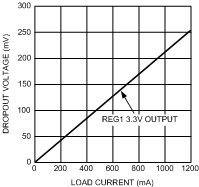
7.14.1 LDO Dropout Voltage vs Load Current Collect Data for all LDOs
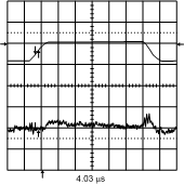
| VIN = 3 V to 4 V | VOUT = 1.8 V | Load = 100 mA |
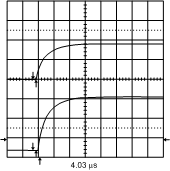
| SYS_ENABLE from 0 | Load (V) = 100 mA | LDO1 Channel 2 | LDO4 Channel 1 |
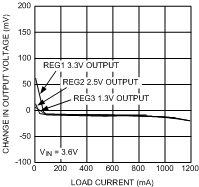
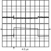
| VIN = 4.1 V | VOUT = 1.8 V | No-Load = 100 mA |
7.14.2 Buck1 Output Efficiency vs. Load Current Varied From 1 mA to 1.5 A
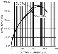
| VIN = 3 V, 3.5 V | VOUT = 1.4 V |
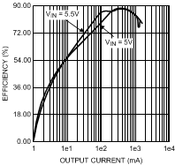
| VIN = 3 V, 3.5 V | VOUT = 1.4 V |
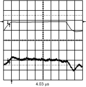
| VIN = 4.1 V | VOUT = 1.4 V | 980 mA [Channel 2] |
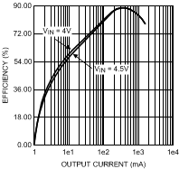
| VIN = 4 V to 4.5 V | VOUT = 1.4 V |
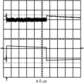
| VIN = 4.1 V | VOUT = 1.4 V (PFM to PWM) | |