SLVSH05 November   2023 LP8865U-Q1 , LP8865V-Q1 , LP8865W-Q1 , LP8865X-Q1 , LP8865Y-Q1 , LP8865Z-Q1

PRODUCTION DATA  

  1.   1
  2. Features
  3. Applications
  4. Description
  5. Comparison Table
  6. Pin Configuration and Functions
  7. Specifications
    1. 6.1 Absolute Maximum Ratings
    2. 6.2 ESD Ratings
    3. 6.3 Recommended Operating Conditions
    4. 6.4 Thermal Information
    5. 6.5 Electrical Characteristics
    6. 6.6 Typical Characteristics
  8. Detailed Description
    1. 7.1 Overview
    2. 7.2 Functional Block Diagram
    3. 7.3 Feature Description
      1. 7.3.1 Adaptive Off-Time Current Mode Control
        1. 7.3.1.1 Switching Frequency Settings
        2. 7.3.1.2 Spread Spectrum
      2. 7.3.2 Setting LED Current
      3. 7.3.3 Internal Soft Start
      4. 7.3.4 Dimming Mode
        1. 7.3.4.1 PWM dimming
        2. 7.3.4.2 Analog dimming
        3. 7.3.4.3 Hybrid Dimming
        4. 7.3.4.4 Flexible Dimming
      5. 7.3.5 Undervoltage Lockout
      6. 7.3.6 Fault Protection
      7. 7.3.7 Thermal Foldback
  9. Application and Implementation
    1. 8.1 Application Information
    2. 8.2 Typical Application
      1. 8.2.1 LP8865XQDMTRQ1 12-V Input, 0.5-A Output, 8-piece LED With Boost Topology
        1. 8.2.1.1 Design Requirements
        2. 8.2.1.2 Detailed Design Procedure
          1. 8.2.1.2.1 Inductor Selection
          2. 8.2.1.2.2 Input Capacitor Selection
          3. 8.2.1.2.3 Output Capacitor Selection
          4. 8.2.1.2.4 Sense Resistor Selection
          5. 8.2.1.2.5 Other External Components Selection
        3. 8.2.1.3 Application Curves
      2. 8.2.2 LP8865YQDMTRQ1 12-V Input, 0.5-A Output, 5-piece LED With Buck-Boost Topology
        1. 8.2.2.1 Design Requirements
        2. 8.2.2.2 Detailed Design Procedure
          1. 8.2.2.2.1 Inductor Selection
          2. 8.2.2.2.2 Input Capacitor Selection
          3. 8.2.2.2.3 Output Capacitor Selection
          4. 8.2.2.2.4 Sense Resistor Selection
          5. 8.2.2.2.5 Other External Components Selection
        3. 8.2.2.3 Application Curves
      3. 8.2.3 LP8865ZQDMTRQ1 12-V Input, 1-A Output, 1-piece LED With Buck Topology
        1. 8.2.3.1 Design Requirements
        2. 8.2.3.2 Detailed Design Procedure
          1. 8.2.3.2.1 Inductor Selection
          2. 8.2.3.2.2 Input Capacitor Selection
          3. 8.2.3.2.3 Output Capacitor Selection
          4. 8.2.3.2.4 Sense Resistor Selection
          5. 8.2.3.2.5 Other External Components Selection
        3. 8.2.3.3 Application Curves
    3. 8.3 Power Supply Recommendations
    4. 8.4 Layout
      1. 8.4.1 Layout Guidelines
      2. 8.4.2 Layout Example
  10. Device and Documentation Support
    1. 9.1 Receiving Notification of Documentation Updates
    2. 9.2 Support Resources
    3. 9.3 Trademarks
    4. 9.4 Electrostatic Discharge Caution
    5. 9.5 Glossary
  11. 10Revision History
  12. 11Mechanical, Packaging, and Orderable Information

パッケージ・オプション

メカニカル・データ(パッケージ|ピン)
サーマルパッド・メカニカル・データ
発注情報

Hybrid Dimming

The LP8865 family supports a unique hybid dimming function to maximize the dimming performance, especially when both high dimming frequency and high dimming ratio are needed. The hybrid dimming mode is enabled when the ADIM/HD pin is always low and the PWM/EN pin is configured by a PWM input signal.

When the hybrid dimming is enabled, the LED current is regulated by the analog dimming at high brightness level (12.5% - 100%) and by the PWM dimming at low brightness level (0% - 12.5%), respectively. At high brightness level, the internal voltage reference, VREF, changes in proportion to the duty cycle of the PWM input signal at the PWM/EN pin. At low brightness level, VREF stays unchanged and an internal PWM generator is enabled. Thus, the LED is turned on and off corresponding to the on and off of the internal PWM signal of which the frequency and the duty cycle are configured by the PWM input signal at the PWM/EN pin. The detailed hybrid dimming behavior is illustrated in the below figure.
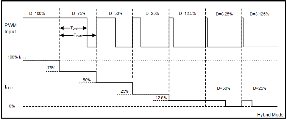
GUID-1485AEB2-3DFC-45E6-9881-FD77A606B92D-low.gif Figure 7-3 Hybrid Dimming