SLES254D April 2010 – July 2015 PCM1753-Q1 , PCM1754-Q1
PRODUCTION DATA.
- 1 Features
- 2 Applications
- 3 Description
- 4 Revision History
- 5 Device Comparison Table
- 6 Pin Configuration Functions
- 7 Specifications
-
8 Detailed Description
- 8.1 Overview
- 8.2 Functional Block Diagram
- 8.3 Feature Description
- 8.4 Device Functional Modes
- 8.5 Programming
- 8.6
Register Maps
- 8.6.1
Mode Control Registers (PCM1753-Q1)
- 8.6.1.1 User-Programmable Mode Controls
- 8.6.1.2
Register Definitions
- 8.6.1.2.1 ATx[7:0]: Digital Attenuation Level Setting
- 8.6.1.2.2 MUTx: Soft Mute Control
- 8.6.1.2.3 OVER: Oversampling Rate Control
- 8.6.1.2.4 SRST: Reset
- 8.6.1.2.5 DACx: DAC Operation Control
- 8.6.1.2.6 DM12: Digital De-Emphasis Function Control
- 8.6.1.2.7 DMF[1:0]: Sampling Frequency Selection for the De-Emphasis Function
- 8.6.1.2.8 FMT[2:0]: Audio Interface Data Format
- 8.6.1.2.9 FLT: Digital Filter Rolloff Control
- 8.6.1.2.10 DREV: Output Phase Select
- 8.6.1.2.11 ZREV: Zero Flag Polarity Select
- 8.6.1.2.12 AZRO: Zero Flag Function Select
- 8.6.1
Mode Control Registers (PCM1753-Q1)
- 9 Application and Implementation
- 10Power Supply Recommendations
- 11Layout
- 12Device and Documentation Support
- 13Mechanical, Packaging, and Orderable Information
8 Detailed Description
8.1 Overview
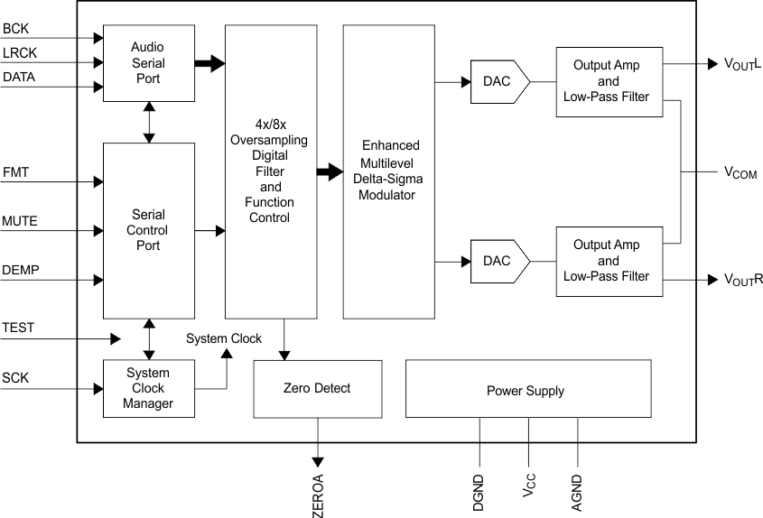
The PCM175x-Q1 family of devices are stereo digital-to-analog converters (DACs) based on TI's enhanced delta-sigma architecture which employs 4th-order noise shaping and 8-level amplitude quantization to achieve excellent dynamic performance and improved clock jitter tolerance. The PCM175x-Q1 family of devices easily interface with an audio DSP and decoder chips because of the device supports industry-standard audio data formats with 16- and 24-bit data. The PCM1754-Q1 device also offers hardware control.
8.2 Functional Block Diagram
8.3 Feature Description
8.3.1 System Clock and Reset Functions
8.3.1.1 System Clock Input
The PCM175x-Q1 family of devices requires a system clock for operating the digital interpolation filters and multilevel delta-sigma modulators. The system clock is applied at the SCK input (pin 16). Table 1 lists examples of system clock frequencies for common audio sampling rates.
Figure 20 shows and the System Clock Input Timing table lists the timing requirements for the system clock input. For optimal performance, use a clock source with low phase-jitter and noise. TI's PLL170x family of multiclock generators is an excellent choice for providing the PCM175x-Q1 system clock.
Table 1. System Clock Rates for Common Audio Sampling Frequencies
| SAMPLING FREQUENCY | SYSTEM CLOCK FREQUENCY (fSCLK) (MHz) | ||||||
|---|---|---|---|---|---|---|---|
| 128 fS | 192 fS | 256 fS | 384 fS | 512 fS | 768 fS | 1152 fS | |
| 8 kHz | 1.024 | 1.536 | 2.048 | 3.072 | 4.096 | 6.144 | 9.216 |
| 16 kHz | 2.048 | 3.072 | 4.096 | 6.144 | 8.192 | 12.288 | 18.432 |
| 32 kHz | 4.096 | 6.144 | 8.192 | 12.288 | 16.384 | 24.576 | 36.864 |
| 44.1 kHz | 5.6448 | 8.4672 | 11.2896 | 16.9344 | 22.5792 | 33.8688 | See (1) |
| 48 kHz | 6.144 | 9.216 | 12.288 | 18.432 | 24.576 | 36.864 | See (1) |
| 88.2 kHz | 11.2896 | 16.9344 | 22.5792 | 33.8688 | 45.1584 | See (1) | See (1) |
| 96 kHz | 12.288 | 18.432 | 24.576 | 36.864 | 49.152 | See (1) | See (1) |
| 192 kHz | 24.576 | 36.864 | See (1) | See (1) | See (1) | See (1) | See (1) |

8.3.1.2 Power-On Reset Functions
The PCM175x-Q1 family of devices includes a power-on reset function. Figure 21 shows the operation of this function. With the system clock active and VCC > 3 V (typical, 2.2 V to 3.7 V), the power-on reset function is enabled. The initialization sequence requires 1024 system clocks from the time VCC > 3 V (typical, 2.2 V to
3.7 V).
During the reset period (1024 system clocks), the analog output is forced to the bipolar zero level, or VCC / 2. After the reset period, an internal register is initialized in the next 1 / fS period and if SCK, BCK, and LRCK are provided continuously, the PCM175x-Q1 family of devices provides proper analog output with unit group delay against the input data.
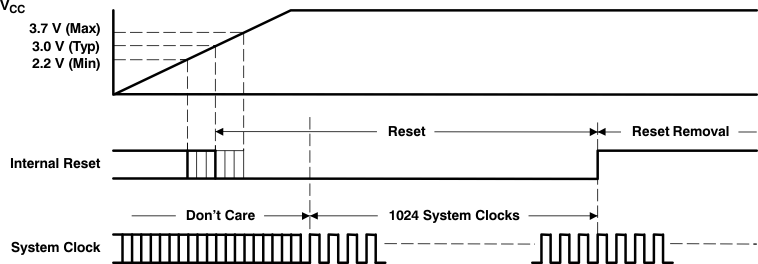 Figure 21. Power-On Reset Timing
8.3.2 Audio Serial Interface
The audio serial interface for the PCM175x-Q1 family of devices consists of a 3-wire synchronous serial port. The interface includes LRCK (pin 3), BCK (pin 1), and DATA (pin 2). The BCK pin is the serial audio bit clock, and is used to clock the serial data present on the DATA pin into the serial shift register of the audio interface. Serial data is clocked into the PCM175x-Q1 family of devices on the rising edge of BCK. The LRCK pin is the serial audio left and right word clock. This pin is used to latch serial data into the internal registers of the serial audio interface.
Both the LRCK and BCK pins should be synchronous to the system clock. Ideally, TI recommends that the LRCK and BCK pins be derived from the system clock input, SCK. The LRCK pin is operated at the sampling frequency, fS. The BCK pin can operate at 32, 48, or 64 times the sampling frequency for standard (right-justified) format, and 32 times the sampling frequency of the BCK pin is limited to 16-bit right-justified format only. The BCK pin can operate at 48 or 64 times the sampling frequency for the I2S and left-justified formats, and 48 times the sampling frequency of the BCK pin is limited to 192, 384, and 768 fS SCKI.
Internal operation of the PCM175x-Q1 family of devices is synchronized with the LRCK pin. Accordingly, internal operation is held when the sampling rate clock of the LRCK pin changes or when the SCK pin, BCK pin, or both pins are interrupted for a 3-bit clock cycle or longer. If the SCK, BCK, and LRCK pins are provided continuously after this held condition, the internal operation is re-synchronized automatically in a period of less than 3 / fS. External resetting is not required.
8.3.2.1 Audio Data Formats and Timing
The PCM1753-Q1 device supports industry-standard audio data formats, including right-justified, I2S, and left-justified. The PCM1754-Q1 device supports I2S and 16-bit-word right-justified audio data formats. Figure 23 shows the data formats. Data formats are selected using the format bits, FMT[2:0], located in control register 20 of the PCM1753-Q1 device, and are selected using the FMT pin on the PCM1754-Q1 device. The default data format is 24-bit left-justified. All formats require binary 2s-complement MSB-first audio data. Figure 22 shows a detailed timing diagram for the serial audio interface. The Audio Interface Timing table lists the audio interface timing requirements.
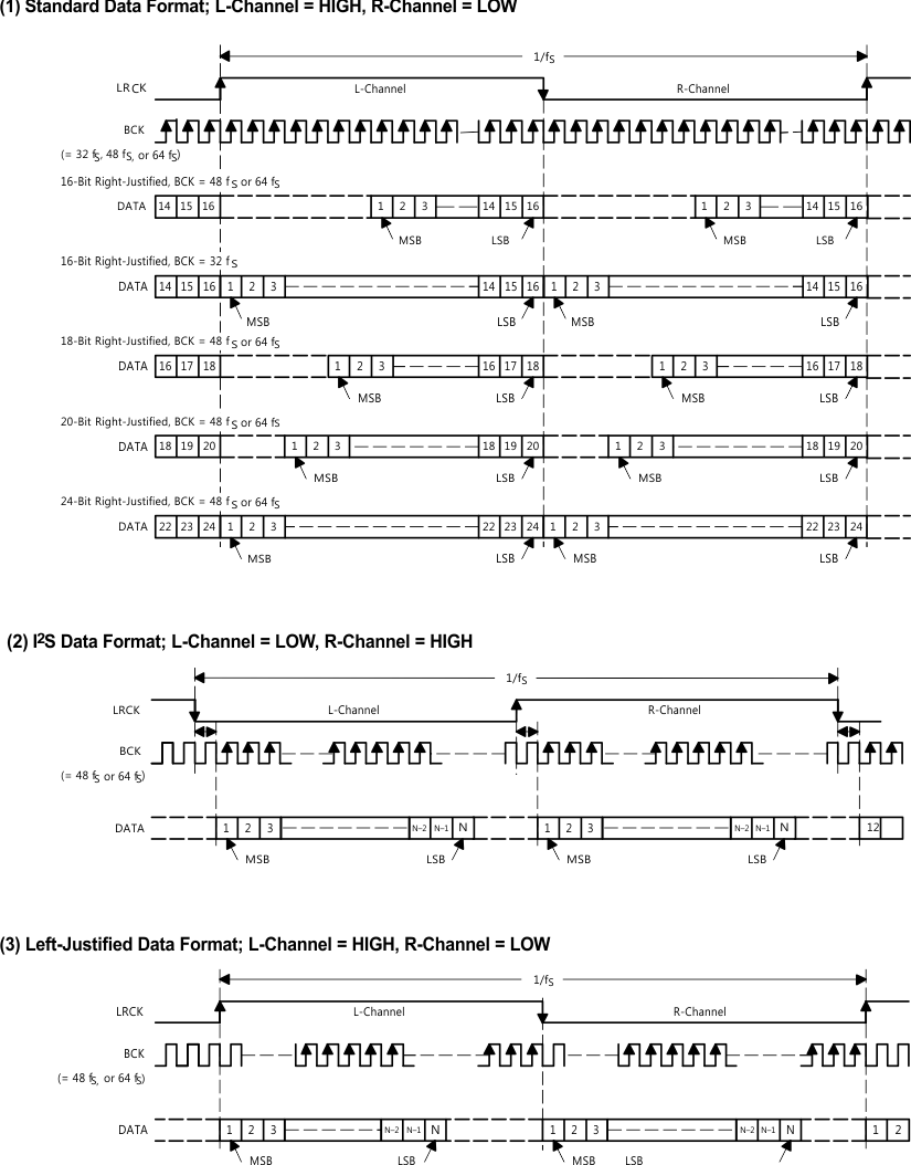 Figure 23. Audio Data Input Formats
8.3.3 Zero Flag (PCM1754-Q1)
The PCM1754-Q1 device has a ZERO flag pin, ZEROA (pin 11). The ZEROA pin is the L-channel and R-channel common zero flag pin. If the data for L-channel and R-channel remains at a 0 level for 1024 sampling periods (or LRCK clock periods), the ZEROA pin is set to a logic 1 state.
8.3.4 Zero Flag (PCM1753-Q1)
Zero-Detect Condition
Zero detection for either output channel is independent from the other channel. If the data for a given channel remains at a 0 level for 1024 sample periods (or LRCK clock periods), a zero-detect condition exists for that channel.
8.3.5 Zero Flag Outputs
If a zero-detect condition exists for one or more channels, the zero flag pins for those channels are set to a logic 1 state. Each channel has zero flag pins, ZEROL (pin 12) and ZEROR (pin 11). These pins can operate external mute circuits, or used as status indicators for a microcontroller, audio signal processor, or other digitally controlled function. The active polarity of the zero flag outputs can be inverted by setting the ZREV bit of control register 22 to 1. The reset default is active-high output, or ZREV set to 0. The L-channel and R-channel common zero flag can be selected by setting the AZRO bit of control register 22 to 1. The reset default is independent zero flags for L-channel and R-channel, or AZRO set to 0.
8.3.6 Analog Outputs
The PCM1753-Q1 device includes two independent output channels, VOUTL and VOUTR. These are unbalanced outputs, each capable of driving 4 VPP typical into a 5-kΩ ac-coupled load. The internal output amplifiers for VOUTL and VOUTR are biased to the dc common-mode (or bipolar zero) voltage, equal to 0.5 VCC.
The output amplifiers include an RC continuous-time filter, which helps to reduce the out-of-band noise energy present at the DAC outputs due to the noise shaping characteristics of the PCM1754-Q1 delta-sigma DAC. The frequency response of this filter is shown in Figure 24. By itself, this filter is not enough to attenuate the out-of-band noise to an acceptable level for many applications. An external low-pass filter is required to provide sufficient out-of-band noise rejection. Further discussion of DAC post-filter circuits is provided in the Applications Information section of this data sheet.
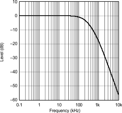 Figure 24. Level vs Frequency
Output Filter Frequency Response
8.3.6.1 VCOM Output
One unbuffered common-mode voltage output pin, VCOM (pin 10) is brought out for decoupling purposes. This pin is nominally biased to a DC-voltage level that is equal to 0.5 VCC. This pin can be used to bias external circuits. Figure 25 shows an example of using the VCOM pin for external biasing applications.
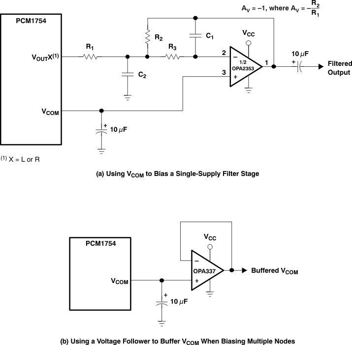 Figure 25. Biasing External Circuits Using the VCOM Pin
8.4 Device Functional Modes
8.4.1 Hardware Control (PCM1754-Q1)
The digital functions of the PCM1754-Q1 device are capable of hardware control. Table 2 lists selectable formats, Table 3 lists de-emphasis control, and Table 4 lists mute control.
Table 2. Data Format Select
| FMT (PIN 15) | DATA FORMAT |
|---|---|
| LOW | 16– to 24–bit, I2S format |
| HIGH | 16–bit right–justified |
Table 3. De-Emphasis Control
| DEMP (PIN 13) | DE–EMPHASIS FUNCTION |
|---|---|
| LOW | 44.1 kHz de–emphasis OFF |
| HIGH | 44.1 kHz de–emphasis ON |
Table 4. Mute Control
| MUTE (PIN 14) | MUTE |
|---|---|
| LOW | Mute OFF |
| HIGH | Mute ON |
8.4.2 Oversampling Rate Control (PCM1754-Q1)
The PCM1754-Q1 device automatically controls the oversampling rate of the delta-sigma DACs with the system clock rate. The oversampling rate is set to 64× oversampling with every system clock and sampling frequency.
8.5 Programming
8.5.1 Software Control (PCM1753-Q1)
The PCM1753-Q1 device has many programmable functions which can be controlled in the software control mode. The functions are controlled by programming the internal registers using ML, MC, and MD.
The serial control interface is a 3-wire serial port, which operates asynchronously to the audio serial interface. The serial control interface is used to program the on-chip mode registers. The control interface includes the MD (pin 13), MC (pin 14), and ML (pin 15) pins. The MD pin is the serial data input, used to program the mode registers. The MC pin is the serial bit clock, used to shift data into the control port. The ML pin is the control port latch clock.
8.5.1.1 Register Write Operation
All write operations for the serial control port use 16-bit data words. Figure 26 shows the control data word format. The most significant bit must be a 0. There are seven bits, labeled IDX[6:0], that set the register index (or address) for the write operation. The least significant eight bits, D[7:0], contain the data to be written to the register specified by IDX[6:0].
Figure 27 shows the functional timing diagram for writing to the serial control port. ML is held at a logic 1 state until a register needs to be written. To begin the register write cycle, ML is set to logic 0. Sixteen clocks are then provided on the MC pin, corresponding to the 16 bits of the control data word on MD. After the sixteenth clock cycle has completed, ML is set to logic 1 to latch the data into the indexed mode control register.
 Figure 26. Control Data Word Format for MD
 Figure 27. Register Write Operation
8.6 Register Maps
8.6.1 Mode Control Registers (PCM1753-Q1)
8.6.1.1 User-Programmable Mode Controls
The PCM1753-Q1 device includes a number of user programmable functions, which are accessed through control registers. The registers are programmed using the serial control interface, which was previously discussed in this data sheet. Table 5 lists the available mode control functions, along with the corresponding reset default conditions and associated register index.
Table 5. User-Programmable Mode Controls
| FUNCTION | RESET DEFAULT | REGISTER | BIT(s) |
|---|---|---|---|
| Digital attenuation control, 0 dB to –63 dB in 0.5-dB steps | 0 dB, no attenuation | 16 and 17 | AT1[7:0], AT2[7:0] |
| Soft mute control | Mute disabled | 18 | MUT[2:0] |
| Oversampling rate control (64 fS or 128 fS) | 64 fS oversampling | 18 | OVER |
| Soft reset control | Reset disabled | 18 | SRST |
| DAC operation control | DAC1 and DAC2 enabled | 19 | DAC[2:1] |
| De-emphasis function control | De-emphasis disabled | 19 | DM12 |
| De-emphasis sample rate selection | 44.1 kHz | 19 | DMF[1:0] |
| Audio data format control | 24-bit left-justified | 20 | FMT[2:0] |
| Digital filter rolloff control | Sharp rolloff | 20 | FLT |
| Zero flag function select | L-, R-channel independent | 22 | AZRO |
| Output phase select | Normal phase | 22 | DREV |
| Zero flag polarity select | High | 22 | ZREV |
The mode control register map is shown in Table 6. Each register includes an index (or address) indicated by the IDX[6:0] bits.
Table 6. Mode Control Register Map(1)
| IDX (B8–B14) | REGISTER | B15 | B14 | B13 | B12 | B11 | B10 | B9 | B8 | B7 | B6 | B5 | B4 | B3 | B2 | B1 | B0 |
|---|---|---|---|---|---|---|---|---|---|---|---|---|---|---|---|---|---|
| 10h | Register 16 | 0 | IDX6 | IDX5 | IDX4 | IDX3 | IDX2 | IDX1 | IDX0 | AT17 | AT16 | AT15 | AT14 | AT13 | AT12 | AT11 | AT10 |
| 11h | Register 17 | 0 | IDX6 | IDX5 | IDX4 | IDX3 | IDX2 | IDX1 | IDX0 | AT27 | AT26 | AT25 | AT24 | AT23 | AT22 | AT21 | AT20 |
| 12h | Register 18 | 0 | IDX6 | IDX5 | IDX4 | IDX3 | IDX2 | IDX1 | IDX0 | SRST | OVER | RSV | RSV | RSV | RSV | MUT2 | MUT1 |
| 13h | Register 19 | 0 | IDX6 | IDX5 | IDX4 | IDX3 | IDX2 | IDX1 | IDX0 | RSV | DMF1 | DMF0 | DM12 | RSV | RSV | DAC2 | DAC1 |
| 14h | Register 20 | 0 | IDX6 | IDX5 | IDX4 | IDX3 | IDX2 | IDX1 | IDX0 | RSV | RSV | FLT | RSV | RSV | FMT2 | FMT1 | FMT0 |
| 16h | Register 22 | 0 | IDX6 | IDX5 | IDX4 | IDX3 | IDX2 | IDX1 | IDX0 | RSV | RSV | RSV | RSV | RSV | AZRO | ZREV | DREV |
8.6.1.2 Register Definitions

8.6.1.2.1 ATx[7:0]: Digital Attenuation Level Setting
With x = 1 or 2, corresponding to the DAC output VOUTL (x = 1) and VOUTR (x = 2).
Default value: 1111 1111b
Each DAC channel (VOUTL and VOUTR) includes a digital attenuation function. The attenuation level can be set from 0 dB to –63 dB in 0.5-dB steps. Changes in attenuator levels are made by incrementing or decrementing one step (0.5 dB) for every 8/fS time internal until the programmed attenuator setting is reached. Alternatively, the attenuation level can be set to infinite attenuation (or mute).
The attenuation data for each channel can be set individually. The attenuation level is set using Equation 1.
where
- ATx[7:0]DEC = 0 through 255.
For ATx[7:0]DEC = 0 through 128, attenuation is set to infinite attenuation.
The table in Figure 28 shows the attenuation levels for various settings.
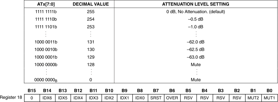 Figure 28. Attenuation Level Settings
8.6.1.2.2 MUTx: Soft Mute Control
With x = 1 or 2, corresponding to the DAC outputs VOUTL (x = 1) and VOUTR (x = 2).
Default value: 0

The mute bits, MUT1 and MUT2, are used to enable or disable the soft mute function for the corresponding DAC outputs, VOUTL and VOUTR. The soft mute function is incorporated into the digital attenuators. When mute is disabled (MUTx = 0), the attenuator and DAC operate normally. When mute is enabled by setting MUTx = 1, the digital attenuator for the corresponding output is decreased from the current setting to infinite attenuation, one attenuator step (0.5 dB) for every 8 / fS seconds. This provides pop-free muting of the DAC output.
By setting MUTx = 0, the attenuator is increased one step for every 8/fS seconds to the previously programmed attenuation level.
8.6.1.2.3 OVER: Oversampling Rate Control
Default value: 0
System clock rate = 256 fS, 384 fS, 512 fS, 768 fS, or 1152 fS:

System clock rate = 128 fS or 192 fS:

The OVER bit is used to control the oversampling rate of the delta-sigma DAC. The OVER = 1 setting is recommended when the sampling rate is 192 kHz (system clock rate is 128 fS or 192 fS).
8.6.1.2.4 SRST: Reset
Default value: 0

The SRST bit is used to enable or disable the soft reset function. The operation is the same as power-on reset. All registers are initialized.

8.6.1.2.5 DACx: DAC Operation Control
With x = 1 or 2, corresponding to the DAC output VOUTL (x = 1) or VOUTR (x = 2).
Default value: 0

The DAC operation controls are used to enable and disable the DAC outputs, VOUTL and VOUTR. When DACx = 0, the corresponding output generates the audio waveform dictated by the data present on the DATA pin. When DACx = 1, the corresponding output is set to the bipolar zero level, or 0.5 VCC.
8.6.1.2.6 DM12: Digital De-Emphasis Function Control
Default value: 0

The DM12 bit is used to enable or disable the digital de-emphasis function. See the plots shown in the Typical Characteristics section of this data sheet.
8.6.1.2.7 DMF[1:0]: Sampling Frequency Selection for the De-Emphasis Function
Default value: 00
The DMF[1:0] bits are used to select the sampling frequency used for the digital de-emphasis function when it is enabled.

8.6.1.2.8 FMT[2:0]: Audio Interface Data Format
Default value: 101
The FMT[2:0] bits are used to select the data format for the serial audio interface. The table in Figure 29 shows the available format options.
 Figure 29. Audio Data Format Options
8.6.1.2.9 FLT: Digital Filter Rolloff Control
Default value: 0

The FLT bit allows the user to select the digital filter rolloff that is best suited to the application. Two filter rolloff selections are available, sharp and slow. The filter responses for these selections are shown in the Typical Characteristics section of this data sheet.

8.6.1.2.10 DREV: Output Phase Select
Default value: 0

The DREV bit is the output analog signal phase control.
8.6.1.2.11 ZREV: Zero Flag Polarity Select
Default value: 01h

The ZREV bit allows the user to select the polarity of zero flag pins.
8.6.1.2.12 AZRO: Zero Flag Function Select
Default value: 0

The AZRO bit allows the user to select the function of zero flag pins.

