JAJS199E April 2003 – July 2019 PCM1753 , PCM1754 , PCM1755
PRODUCTION DATA.
- 1 特長
- 2 アプリケーション
- 3 概要
- 4 改訂履歴
- 5 Device Comparison Table
- 6 Pin Configuration and Functions
- 7 Specifications
-
8 Detailed Description
- 8.1 Overview
- 8.2 Functional Block Diagram
- 8.3 Feature Description
- 8.4 Device Functional Modes
- 8.5 Programming
- 8.6
Register Maps
- 8.6.1
Mode Control Registers (PCM1753/55)
- 8.6.1.1 User-Programmable Mode Controls
- 8.6.1.2
Register Definitions
- 8.6.1.2.1 ATx[7:0]: Digital Attenuation Level Setting
- 8.6.1.2.2 MUTx: Soft Mute Control
- 8.6.1.2.3 OVER: Oversampling Rate Control
- 8.6.1.2.4 SRST: Reset
- 8.6.1.2.5 DACx: DAC Operation Control
- 8.6.1.2.6 DM12: Digital De-Emphasis Function Control
- 8.6.1.2.7 DMF[1:0]: Sampling Frequency Selection for the De-Emphasis Function
- 8.6.1.2.8 FMT[2:0]: Audio Interface Data Format
- 8.6.1.2.9 FLT: Digital Filter Rolloff Control
- 8.6.1.2.10 DREV: Output Phase Select
- 8.6.1.2.11 ZREV: Zero Flag Polarity Select
- 8.6.1.2.12 AZRO: Zero Flag Function Select
- 8.6.1
Mode Control Registers (PCM1753/55)
- 9 Application and Implementation
- 10Power Supply Recommendations
- 11Layout
- 12デバイスおよびドキュメントのサポート
- 13メカニカル、パッケージ、および注文情報
9.2.2.1 Total Harmonic Distortion + Noise
Total harmonic distortion + noise (THD+N) is a significant figure of merit for audio D/A converters because it takes into account both harmonic distortion and all noise sources within a specified measurement bandwidth. The average value of the distortion and noise is referred to as THD+N.
For the PCM175x, THD+N is measured with a full-scale, 1-kHz digital sine wave as the test stimulus at the input of the DAC (see Figure 33). The digital generator is set to 24-bit audio word length and a sampling frequency of 44.1 kHz or 96 kHz. The digital generator output is taken from the unbalanced S/PDIF connector of the measurement system. The S/PDIF data is transmitted via a coaxial cable to the digital audio receiver on the DEM-DAI1753 demonstration board. The receiver is then configured to output 24-bit data in either I2S or left-justified data format. The DAC audio interface format is programmed to match the receiver output format. The analog output is then taken from the DAC post filter and connected to the analog analyzer input of the measurement system. The analog input is band limited using filters resident in the analyzer. The resulting THD+N is measured by the analyzer and displayed by the measurement system.
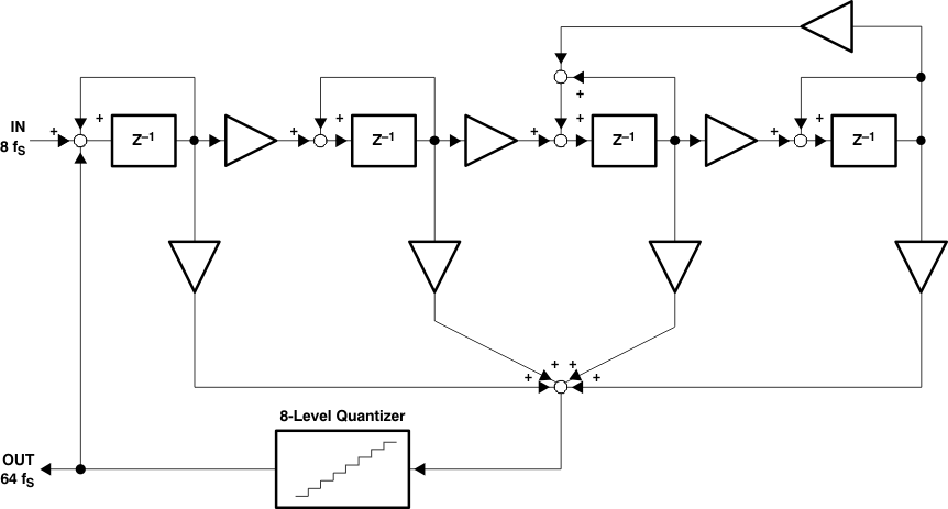
 Figure 32. Eight-Level Delta-Sigma Modulator