SBOS697A September 2014 – January 2017 REF1925 , REF1930 , REF1933 , REF1941
PRODUCTION DATA.
- 1 Features
- 2 Applications
- 3 Description
- 4 Revision History
- 5 Device Comparison Table
- 6 Pin Configuration and Functions
- 7 Specifications
- 8 Parameter Measurement Information
- 9 Detailed Description
- 10Applications and Implementation
- 11Power-Supply Recommendations
- 12Layout
- 13Device and Documentation Support
- 14Mechanical, Packaging, and Orderable Information
10 Applications and Implementation
NOTE
Information in the following applications sections is not part of the TI component specification, and TI does not warrant its accuracy or completeness. TI’s customers are responsible for determining suitability of components for their purposes. Customers should validate and test their design implementation to confirm system functionality.
10.1 Application Information
The low-drift, bidirectional, single-supply, low-side, current-sensing solution described in this section can accurately detect load currents from –2.5 A to 2.5 A. The linear range of the output is from 250 mV to 2.75 V. Positive current is represented by output voltages from 1.5 V to 2.75 V, whereas negative current is represented by output voltages from 250 mV to 1.5 V. The difference amplifier is the INA213 current-shunt monitor, whose supply and reference voltages are supplied by the low-drift REF1930.
10.2 Typical Application
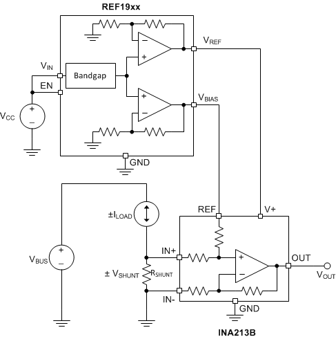
 Figure 45. Low-Side, Current-Sensing Application
10.2.1 Design Requirements
The design requirements are as follows:
- Supply voltage: 5.0 V
- Load current: ±2.5 A
- Output: 250 mV to 2.75 V
- Maximum shunt voltage: ±25 mV
10.2.2 Detailed Design Procedure
Low-side current sensing is desirable because the common-mode voltage is near ground. Therefore, the current-sensing solution is independent of the bus voltage, VBUS. When sensing bidirectional currents, use a differential amplifier with a reference pin. This procedure allows for the differentiation between positive and negative currents by biasing the output stage such that it can respond to negative input voltages. There are a variety of methods for supplying power (V+) and the reference voltage (VREF, or VBIAS) to the differential amplifier. For a low-drift solution, use a monolithic reference that supplies both power and the reference voltage. Figure 46 shows the general circuit topology for a low-drift, low-side, bidirectional, current-sensing solution. This topology is particularly useful when interfacing with an ADC; see Figure 45. Not only do VREF and VBIAS track over temperature, but their matching is much better than alternate topologies. For a more detailed version of the design procedure, refer to TIDU357.
 Figure 46. Low-Drift, Low-side, Bidirectional, Current-Sensing Circuit Topology
The transfer function for the circuit given in Figure 46 is as shown in Equation 5:

10.2.2.1 Shunt Resistor
As illustrated in Figure 46, the value of VSHUNT is the ground potential for the system load. If the value of VSHUNT is too large, issues may arise when interfacing with systems whose ground potential is actually 0 V. Also, a value of VSHUNT that is too negative may violate the input common-mode voltage of the differential amplifier in addition to potential interfacing issues. Therefore, limiting the voltage across the shunt resistor is important. Equation 6 can be used to calculate the maximum value of RSHUNT.

Given that the maximum shunt voltage is ±25 mV and the load current range is ±2.5 A, the maximum shunt resistance is calculated as shown in Equation 7.

To minimize errors over temperature, select a low-drift shunt resistor. To minimize offset error, select a shunt resistor with the lowest tolerance. For this design, the Y14870R01000B9W resistor is used.
10.2.2.2 Differential Amplifier
The differential amplifier used for this design must have the following features:
- Single supply (3 V),
- Reference voltage input,
- Low initial input offset voltage (VOS),
- Low-drift,
- Fixed gain, and
- Low-side sensing (input common-mode range below ground).
For this design, a current-shunt monitor (INA213) is used. The INA21x family topology is shown in Figure 47. The INA213B specifications can be found in the INA213 product data sheet.
 Figure 47. INA21x Current-Shunt Monitor Topology
The INA213B is an excellent choice for this application because all the required features are included. In general, instrumentation amplifiers (INAs) do not have the input common-mode swing to ground that is essential for this application. In addition, INAs require external resistors to set their gain, which is not desirable for low-drift applications. Difference amplifiers typically have larger input bias currents, which reduce solution accuracy at small load currents. Difference amplifiers typically have a gain of 1 V/V. When the gain is adjustable, these amplifiers use external resistors that are not conducive to low-drift applications.
10.2.2.3 Voltage Reference
The voltage reference for this application must have the following features:
- Dual output (3.0 V and 1.5 V),
- Low drift, and
- Low tracking errors between the two outputs.
For this design, the REF1930 is used. The REF19xx topology is as shown in the Functional Block Diagram section.
The REF1930 is an excellent choice for this application because of its dual output. The temperature drift of
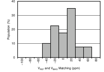
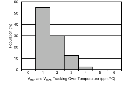
25 ppm/°C and initial accuracy of 0.1% make the errors resulting from the voltage reference minimal in this application. In addition, there is minimal mismatch between the two outputs and both outputs track very well across temperature, as shown in Figure 48 and Figure 49.
 Figure 48. VREF – 2 × VBIAS Distribution (At TA = 25°C)
 Figure 49. Distribution of VREF – 2 × VBIAS Drift Tracking Over Temperature
10.2.2.4 Results
Table 1 summarizes the measured results.
Table 1. Measured Results
| ERROR | UNCALIBRATED (%) | CALIBRATED (%) |
|---|---|---|
| Error across the full load current range (25°C) | ±0.0355 | ±0.004 |
| Error across the full load current range (–40°C to 125°C) | ±0.0522 | ±0.0606 |
10.2.3 Application Curves
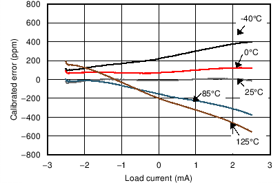
Performing a two-point calibration at 25°C removes the errors associated with offset voltage, gain error, and so forth. Figure 50 to Figure 52 show the measured error at different conditions. For a more detailed description on measurement procedure, calibration, and calculations, please refer to TIDU357.
 Figure 50. Measured Transfer Function
 Figure 52. Calibrated Error vs Load Current
 Figure 51. Uncalibrated Error vs Load Current