SBOS392H August 2007 – August 2019 REF3312 , REF3318 , REF3320 , REF3325 , REF3330 , REF3333
PRODUCTION DATA.
- 1 Features
- 2 Applications
- 3 Description
- 4 Revision History
- 5 Device Comparison
- 6 Pin Configuration and Functions
- 7 Specifications
- 8 Parameter Measurement Information
- 9 Detailed Description
-
10Applications and Implementation
- 10.1 Application Information
- 10.2
Typical Applications
- 10.2.1
REF3312 in a Bipolar Signal-Chain Configuration
- 10.2.1.1 Design Requirements
- 10.2.1.2 Detailed Design Procedure
- 10.2.1.3 Application Curves
- 10.2.1
REF3312 in a Bipolar Signal-Chain Configuration
- 11Power-Supply Recommendations
- 12Layout
- 13Device and Documentation Support
- 14Mechanical, Packaging, and Orderable Information
パッケージ・オプション
メカニカル・データ(パッケージ|ピン)
サーマルパッド・メカニカル・データ
発注情報
10.2.1 REF3312 in a Bipolar Signal-Chain Configuration
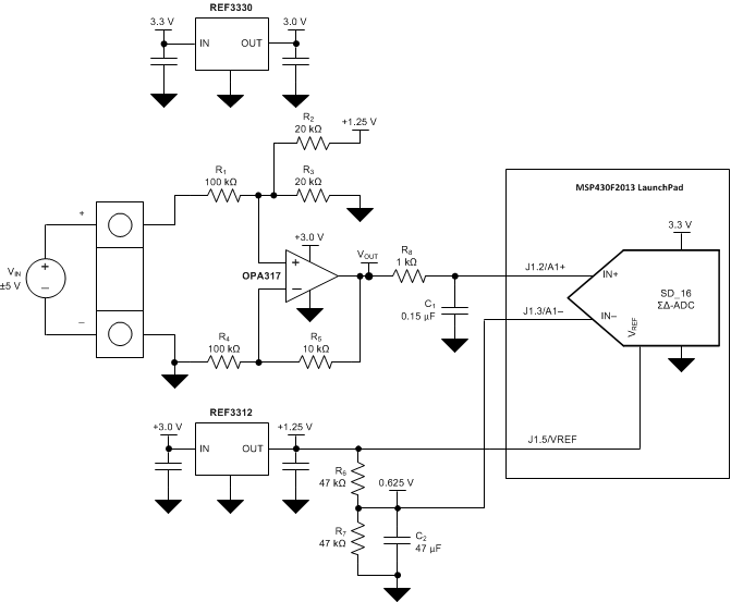
The circuit in Figure 19 consists of a low-power reference and conditioning circuit. This circuit attenuates and level-shifts a bipolar input voltage within the proper input range of a single-supply, low-power, 16-bit ΔΣ analog-to-digital converter (ADC), such as the one inside the MSP430 (or other similar single-supply ADCs). Precision reference circuits are used to level-shift the input signal, provide the ADC reference voltage, and create a well-regulated supply voltage for the low-power analog circuitry. A low-power, zero-drift op amp circuit is used to attenuate and level-shift the input signal.
 Figure 19. Bipolar Signal-Chain Configuration