JAJSPZ6F May 2002 – March 2023 SN65HVD05 , SN65HVD06 , SN65HVD07 , SN75HVD05 , SN75HVD06 , SN75HVD07
PRODUCTION DATA
- 1 特長
- 2 アプリケーション
- 3 概要
- 4 Revision History
-
5 Specifications
- 5.1 Absolute Maximum Ratings
- 5.2 Recommended Operating Conditions
- 5.3 Thermal Information
- 5.4 Package Dissipation Ratings
- 5.5 Driver Electrical Characteristics
- 5.6 Driver Switching Characteristics
- 5.7 Receiver Electrical Characteristics
- 5.8 Receiver Switching Characteristics
- 5.9 Typical Characteristics
- 6 Function Tables
- 7 Equivalent Input and Output Schematic Diagrams
- 8 Application and Implementation
- 9 Device and Documentation Support
- 10Mechanical, Packaging, and Orderable Information
パッケージ・オプション
メカニカル・データ(パッケージ|ピン)
サーマルパッド・メカニカル・データ
発注情報
5.9 Typical Characteristics
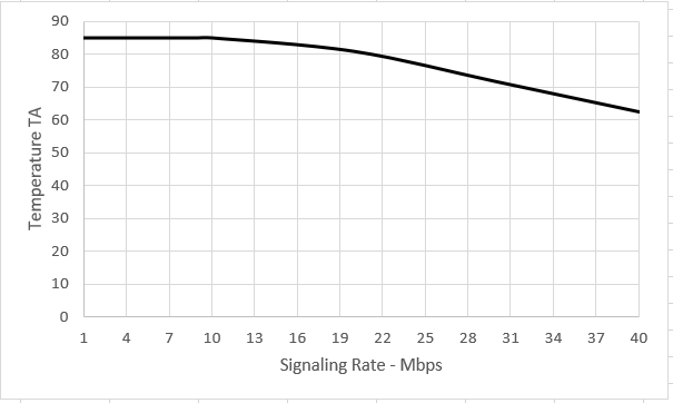 Figure 5-1 HVD05 Maximum Recommended
Still-Air Operating Temperature vs Signaling Rate (D-Package)
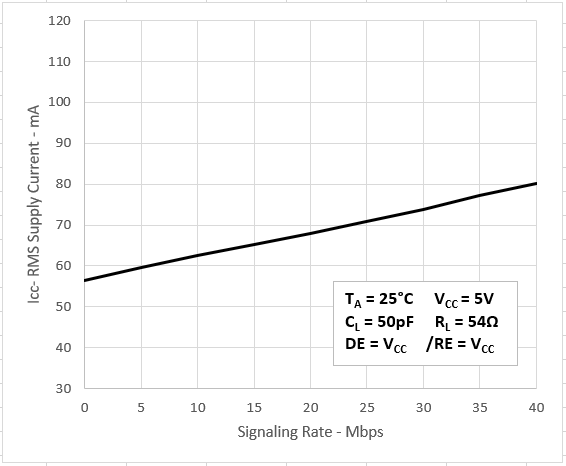 Figure 5-3 HVD05 RMS Supply Current
vs Signaling Rate
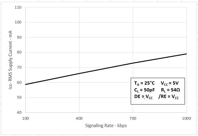 Figure 5-5 HVD07 RMS Supply Current
vs Signaling Rate
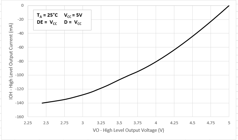 Figure 5-7 Driver High-Level Output
Current vs High-Level Output Voltage
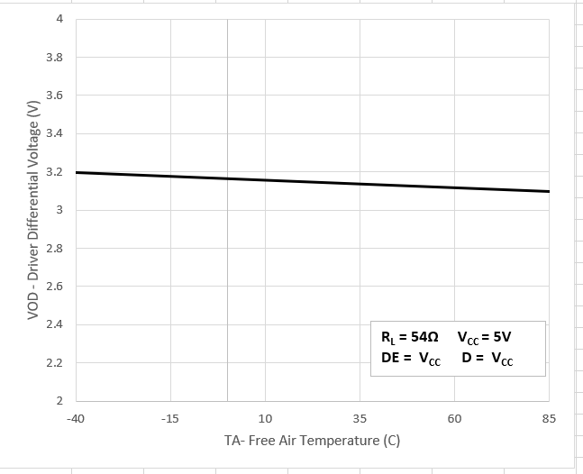 Figure 5-9 Differential Output
Voltage vs Free-Air Temperature
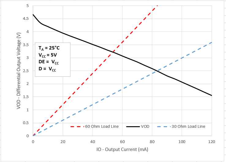 Figure 5-11 Differential Output
Voltage vs Differential Output Current
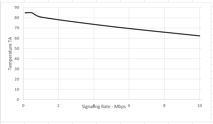 Figure 5-2 HVD06 Maximum Recommended
Still-Air Operating Temperature vs Signaling Rate (D-Package)
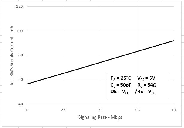 Figure 5-4 HVD06 RMS Supply Current
vs Signaling Rate
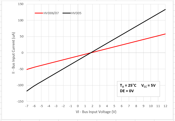 Figure 5-6 BUS Input Current vs BUS
Input Voltage
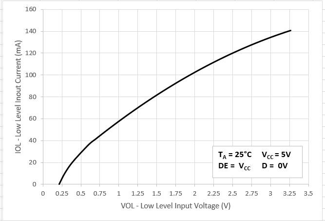 Figure 5-8 Driver Low-Level Output
Current vs Low-Level Output Voltage
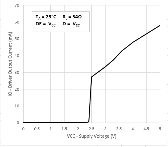 Figure 5-10 Driver Output Current vs
Supply Voltage
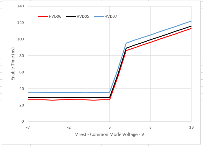 Figure 5-12 Enable Time vs Common-Mode
Voltage
Figure 5-12 Enable Time vs Common-Mode
Voltage(See Figure 5-13)
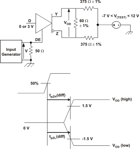 Figure 5-13 Driver Enable Time From DE to VOD