JAJSGX8C April 2002 – February 2019 SN65LVDT14 , SN65LVDT41
PRODUCTION DATA.
- 1 特長
- 2 アプリケーション
- 3 概要
- 4 改訂履歴
- 5 概要(続き)
- 6 Pin Configuration and Functions
-
7 Specifications
- 7.1 Absolute Maximum Ratings
- 7.2 ESD Ratings
- 7.3 Recommended Operating Conditions
- 7.4 Thermal Information
- 7.5 Receiver Electrical Characteristics
- 7.6 Driver Electrical Characteristics
- 7.7 Device Electrical Characteristics
- 7.8 Receiver Switching Characteristics
- 7.9 Driver Switching Characteristics
- 7.10 Typical Characteristics
- 8 Parameter Measurement Information
- 9 Detailed Description
- 10Application and Implementation
- 11Power Supply Recommendations
- 12Layout
- 13デバイスおよびドキュメントのサポート
- 14メカニカル、パッケージ、および注文情報
パッケージ・オプション
デバイスごとのパッケージ図は、PDF版データシートをご参照ください。
メカニカル・データ(パッケージ|ピン)
- PW|20
サーマルパッド・メカニカル・データ
発注情報
8 Parameter Measurement Information
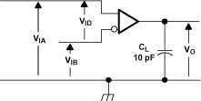
 Figure 8. Receiver Voltage Definitions
 Table 1. Receiver Minimum and Maximum Input Threshold Test Voltages
| APPLIED VOLTAGES | RESULTING DIFFERENTIAL
INPUT VOLTAGE |
RESULTING
COMMON-MODE INPUT VOLTAGE |
|
|---|---|---|---|
| VIA | VIB | VID | VIC |
| 1.25 V | 1.15 V | 100 mV | 1.2 V |
| 1.15 V | 1.25 V | –100 mV | 1.2 V |
| 2.4 V | 2.3 V | 100 mV | 2.35 V |
| 2.3 V | 2.4 V | –100 mV | 2.35 V |
| 0.1 V | 0.0 V | 100 mV | 0.05 V |
| 0.0 V | 0.1 V | –100 mV | 0.05 V |
| 1.5 V | 0.9 V | 600 mV | 1.2 V |
| 0.9 V | 1.5 V | –600 mV | 1.2 V |
| 2.4 V | 1.8 V | 600 mV | 2.1 V |
| 1.8 V | 2.4 V | –600 mV | 2.1 V |
| 0.6 V | 0.0 V | 600 mV | 0.3 V |
| 0.0 V | 0.6 V | –600 mV | 0.3 V |
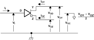
 Figure 9. Driver Voltage and Current Definitions
  Figure 10. Receiver Timing Test Circuit
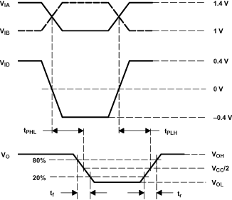
A. All input pulses are supplied by a generator having the following characteristics: tr or tf ≤ 1 ns, pulse repetition rate (PRR) = 1 Mpps, pulse width = 0.5 ± 0.05 µs. CL includes instrumentation and fixture capacitance within 0,06 m of the D.U.T.
Figure 11. Receiver Timing Test Circuit Waveforms  Figure 12. Driver VDO Test Circuit
A. All input pulses are supplied by a generator having the following characteristics: tr or tf ≤ 1 ns, pulse repetition rate (PRR) = 0.5 Mpps, pulse width = 500 ± 10 ns. CL includes instrumentation and fixture capacitance within 0.06 mm of the D.U.T. The measurement of VOC(PP) is made on test equipment with a –3-dB bandwidth of at least 1 GHz.
Figure 13. Test Circuit and Definitions for the Driver Common-Mode Output Voltage 
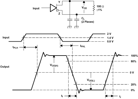
A. All input pulses are supplied by a generator having the following characteristics: tr or tf ≤ 1 ns, pulse repetition rate (PRR) = 1 Mpps, pulse width = 0.5 ± 0.05 µs. CL includes instrumentation and fixture capacitance within 0.06 mm of the D.U.T.
Figure 14. Test Circuit, Timing, and Voltage Definitions for the Differential Output Signal