SCLS746A February 2014 – October 2014 SN74GTL2014
PRODUCTION DATA.
- 1 Features
- 2 Applications
- 3 Description
- 4 Revision History
- 5 Pin Configuration and Functions
- 6 Specifications
- 7 Parameter Measurement Information
- 8 Detailed Description
- 9 Application and Implementation
- 10Power Supply Recommendations
- 11Layout
- 12Device and Documentation Support
- 13Mechanical, Packaging, and Orderable Information
9 Application and Implementation
NOTE
Information in the following applications sections is not part of the TI component specification, and TI does not warrant its accuracy or completeness. TI’s customers are responsible for determining suitability of components for their purposes. Customers should validate and test their design implementation to confirm system functionality.
9.1 Application Information
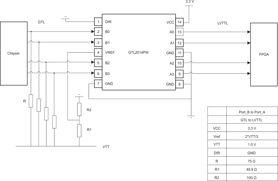
GTL2014 is the voltage translator for GTL–/GTL/GTL+ to LVTTL or LVTTL to GTL–/GTL/GTL+. Please find the reference schematic and recommend value for passive component in the Typical Application.
9.2 Typical Application
9.2.1 GTL–/GTL/GTL+ to LVTTL
Select appropriate VTT/VREF based upon GTL–/GTL/GTL+. The parameters in Recommended Operating Conditions are compliant to the GTL specification.
9.2.1.1 Design Requirements
The GTL2014 requires industrial standard LVTTL and GTL inputs. The design example in Application Information show standard voltage level and typical resistor values.
NOTE
Only LVTTL terminals (A1/A2/A3/A4) are tolerant to 5 V.
9.2.1.2 Detailed Design Procedure
To begin the design process, determine the following:
- Select direction base upon application (GTL–/GTL/GTL+ to LVTTL or LVTTL to GTL–/GTL/GTL+).
- Set up appropriate DIR pin and VREF/VTT.
- Choose correct pullup resistor value base upon data rate and driving current requirement (for LVTTL to GTL–/GTL/GTL+).
9.2.1.3 Application Curve
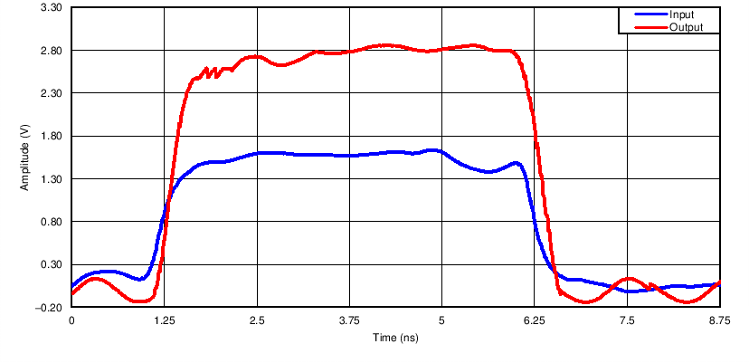
 Figure 6. GTL-to-LVTTL, VREF = 1 V, VIN = 1.5 V, 100 MHz
9.2.2 LVTTL/TTL to GTL–/GTL/GTL+
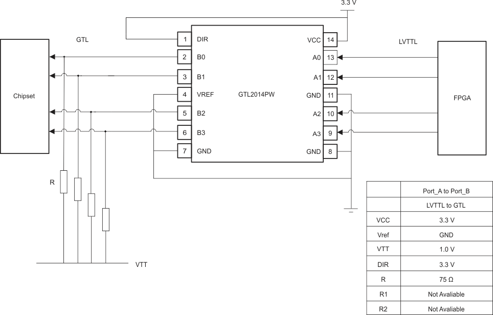
Because GTL is an open-drain interface, the selection of pullup resistor depends on the application requirement (for example, data rate) and PCB trace capacitance.
 Figure 7. Application Diagram for LVTTL to GTL
9.2.2.1 Design Requirements
The GTL2014 requires industrial standard LVTTL and GTL inputs. The design example in the Application Information section show standard voltage level and typical resistor values.
NOTE
Only LVTTL terminals (A1/A2/A3/A4) are tolerant to 5 V.
9.2.2.2 Detailed Design Procedure
To begin the design process, determine the following:
- Select direction based upon application (GTL–/GTL/GTL+ to LVTTL or LVTTL to GTL–/GTL/GTL+).
- Set up appropriate DIR pin and VREF/VTT.
- Choose correct pullup resistor value base upon data rate and driving current requirement (for LVTTL to GTL–/GTL/GTL+).
9.2.2.3 Application Curve
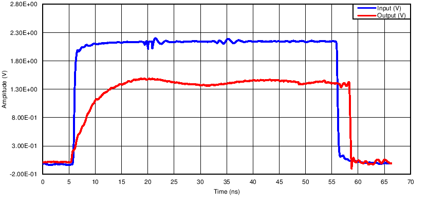
 Figure 8. LVTTL-to-GTL, VREF = 1 V, VTT = 1.5 V, 10 MHz
