JAJSUB4F July 1993 – April 2024 SN65LBC172 , SN75LBC172
PRODUCTION DATA
- 1
- 1 特長
- 2 アプリケーション
- 3 概要
- 4 Pin Configuration and Functions
- 5 Specifications
- 6 Parameter Measurement Information
- 7 Detailed Description
- 8 Device and Documentation Support
- 9 Revision History
- 10Mechanical, Packaging, and Orderable Information
パッケージ・オプション
デバイスごとのパッケージ図は、PDF版データシートをご参照ください。
メカニカル・データ(パッケージ|ピン)
- N|16
- DW|20
サーマルパッド・メカニカル・データ
発注情報
5.7 Typical Characteristics
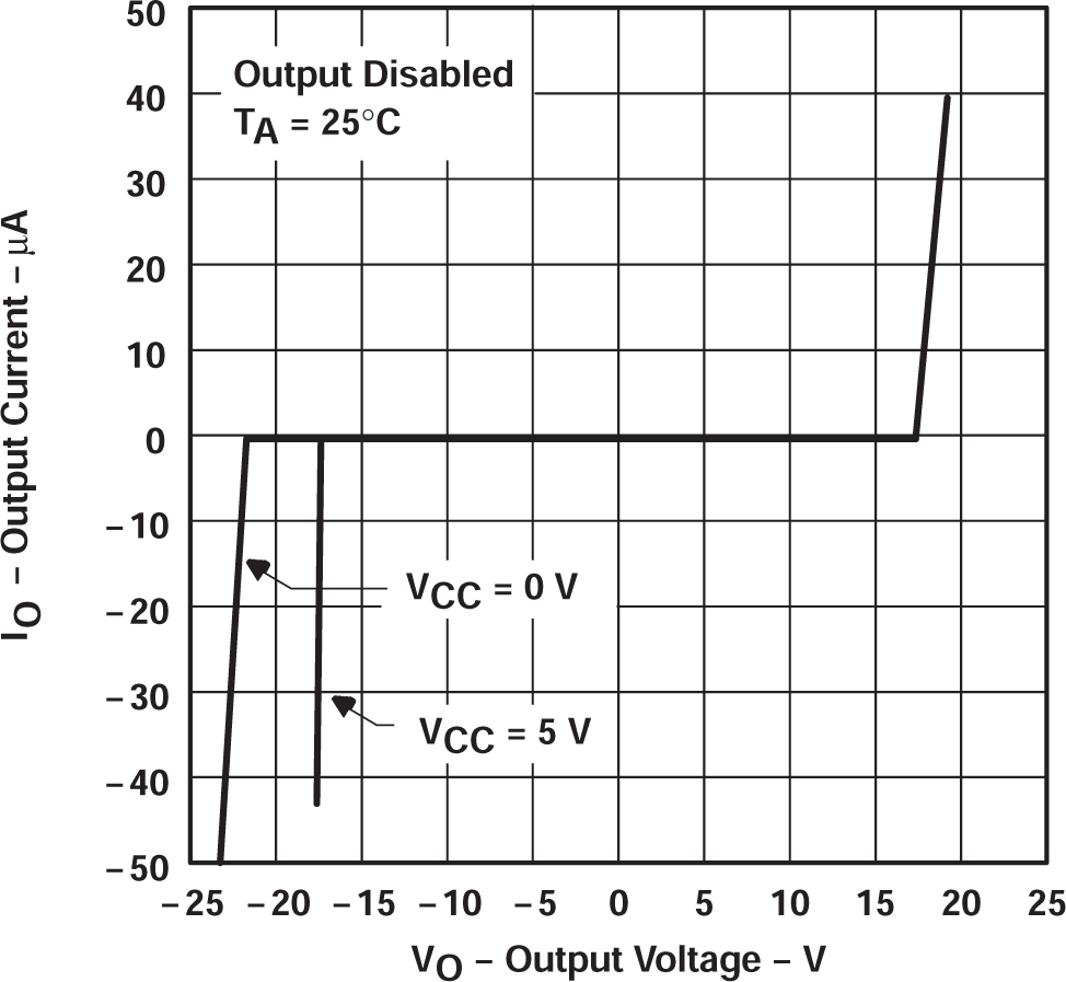 Figure 5-1 Output Current vs Output
Voltage
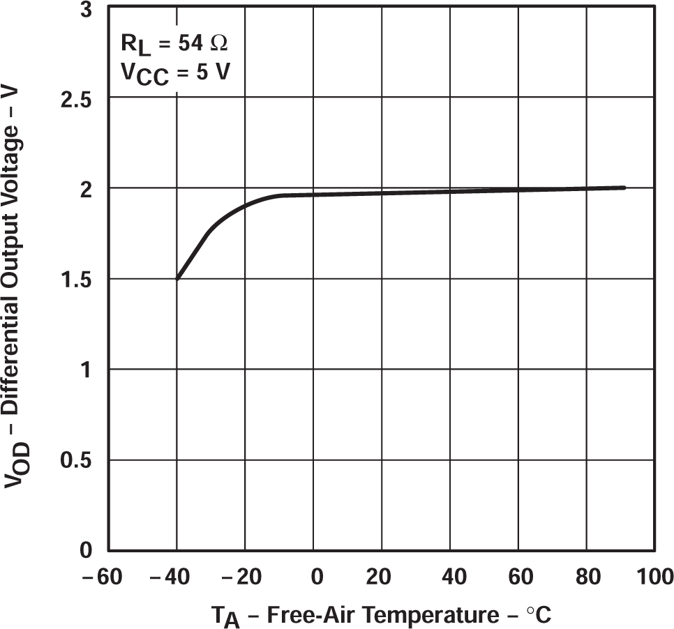 Figure 5-3 Differential Output
Voltage vs Free-air Temperature
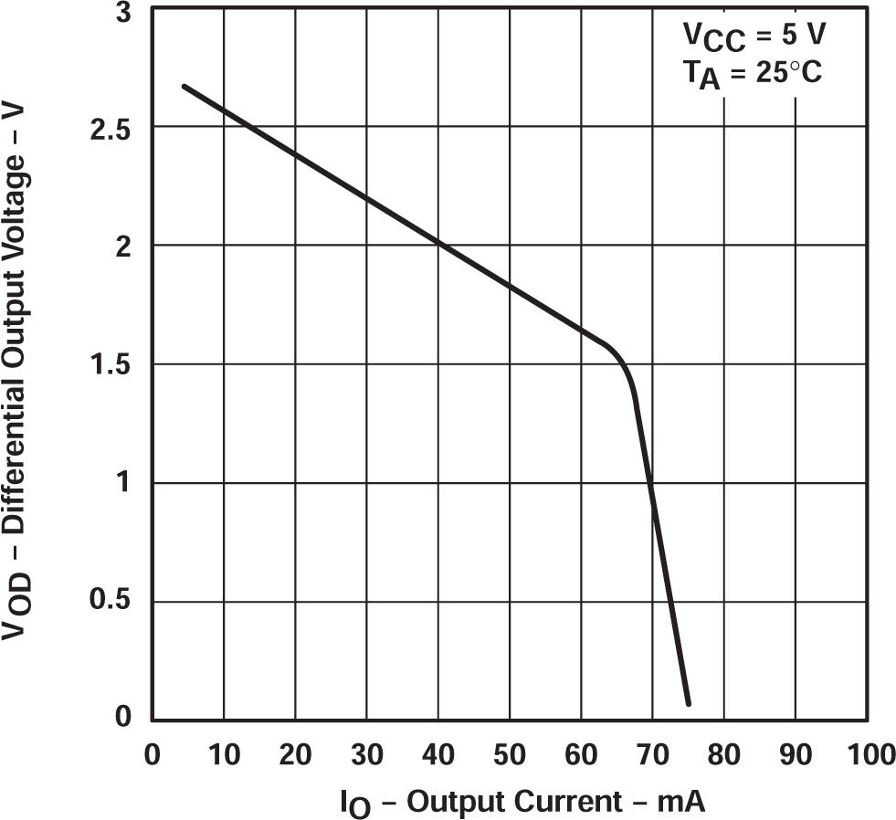 Figure 5-5 Differential Output
Voltage vs Output Current
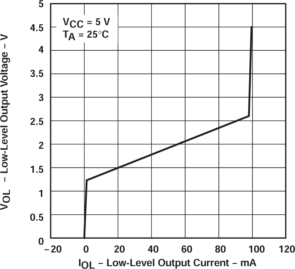 Figure 5-2 Low-level Output Voltage
vs Low-level Output Current
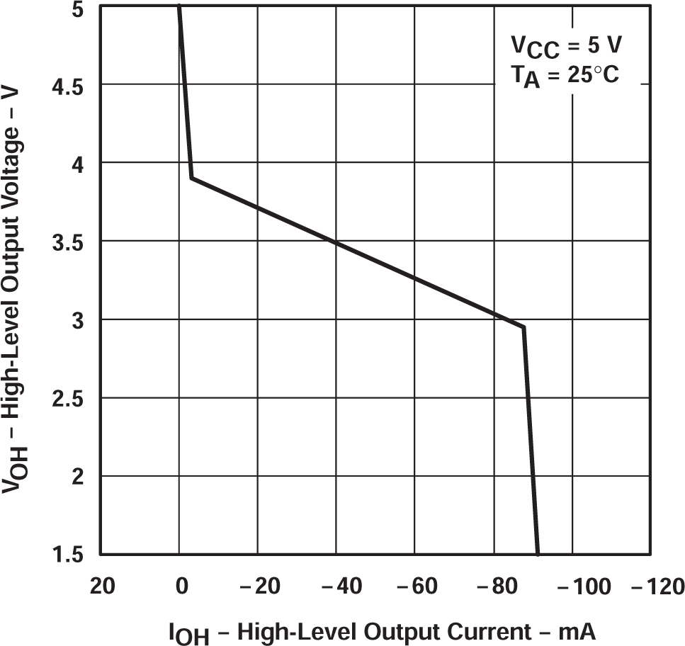 Figure 5-4 High-level Output Voltage
vs High-level Output Current
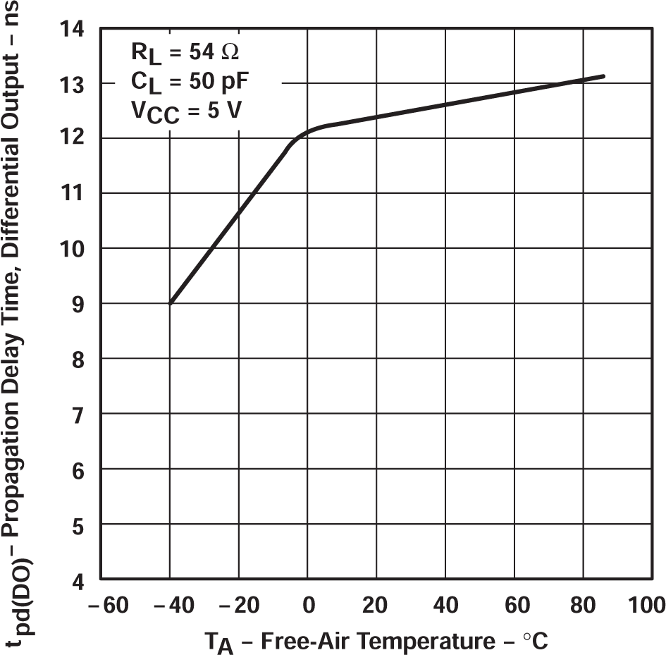 Figure 5-6 Propagation Delay Time,
Differential Output vs Free-air Temperature