JAJSDS3C September 2017 – December 2018 THVD1510 , THVD1512 , THVD1550 , THVD1551 , THVD1552
PRODUCTION DATA.
- 1 特長
- 2 アプリケーション
- 3 概要
- 4 改訂履歴
- 5 Device Comparison Table
- 6 Pin Configuration and Functions
- 7 Specifications
- 8 Parameter Measurement Information
- 9 Detailed Description
- 10Application and Implementation
- 11Power Supply Recommendations
- 12Layout
- 13デバイスおよびドキュメントのサポート
- 14メカニカル、パッケージ、および注文情報
パッケージ・オプション
デバイスごとのパッケージ図は、PDF版データシートをご参照ください。
メカニカル・データ(パッケージ|ピン)
- D|8
- DGK|8
サーマルパッド・メカニカル・データ
発注情報
10.2.1.5 Transient Protection
The bus pins of the THVD15xx transceiver family include on-chip ESD protection against ±30-kV HBM and ±18-kV IEC 61000-4-2 contact discharge. The International Electrotechnical Commission (IEC) ESD test is far more severe than the HBM ESD test. The 50% higher charge capacitance, C(S), and 78% lower discharge resistance, R(D), of the IEC model produce significantly higher discharge currents than the HBM model. As stated in the IEC 61000-4-2 standard, contact discharge is the preferred transient protection test method.
 Figure 25. HBM and IEC ESD Models and Currents in Comparison (HBM Values in Parenthesis)
 The on-chip implementation of IEC ESD protection significantly increases the robustness of equipment. Common discharge events occur because of human contact with connectors and cables. Designers may choose to implement protection against longer duration transients, typically referred to as surge transients.
EFTs are generally caused by relay-contact bounce or the interruption of inductive loads. Surge transients often result from lightning strikes (direct strike or an indirect strike which induce voltages and currents), or the switching of power systems, including load changes and short circuit switching. These transients are often encountered in industrial environments, such as factory automation and power-grid systems.
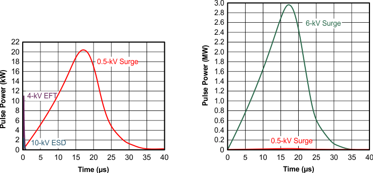
Figure 26 compares the pulse power of the EFT and surge transients with the power caused by an IEC ESD transient. The left-hand diagram shows the relative pulse-power for a 0.5-kV surge transient and 4-kV EFT transient, both of which dwarf the 10-kV ESD transient visible in the lower-left corner. 500-V surge transients are representative of events that may occur in factory environments in industrial and process automation.
The right-hand diagram shows the pulse-power of a 6-kV surge transient, relative to the same 0.5-kV surge transient. 6-kV surge transients are most likely to occur in power generation and power-grid systems.
 Figure 26. Power Comparison of ESD, EFT, and Surge Transients
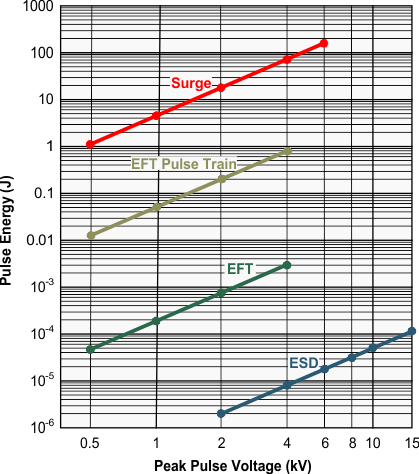
 In the case of surge transients, high-energy content is characterized by long pulse duration and slow decaying pulse power. The electrical energy of a transient that is dumped into the internal protection cells of a transceiver is converted into thermal energy, which heats and destroys the protection cells, thus destroying the transceiver. Figure 27 shows the large differences in transient energies for single ESD, EFT, surge transients, and an EFT pulse train that is commonly applied during compliance testing.
 Figure 27. Comparison of Transient Energies